This thread has been locked.

If you have a related question, please click the "Ask a related question" button in the top right corner. The newly created question will be automatically linked to this question.

CD4504B not working when Vcc = 0V ??

Other Parts Discussed in Thread: CD4504B

Dear Experts,

I'm using a CD4504B level shifter to translate 5V signals to 12V.
However, the 5V power supply is not always present...
... and I have the impression that the device is doing stupid things (high power consumption, and output switching unexpectedly (at least it happened once...)).

Inputs are also not powered, but I have pull-downs on all the inputs, so I presume they should not disturb the CD4504B, but I can find no information about what is supposed to happen when VCC = 0 and VDD = 12V...

Does anyone know?

Thanks for your help!

  • Maybe my question is stupid, but there is no information in the data sheet... What are we supposed to do in this case?

  • Hi,

    The issues are wired. I take some samples to test it and will ask help from design team. When I get feedback I will let you know.

    The input is pulled down when VCC=0. Dose the pull-down resistor is used or connet input to ground directly?

    Thanks


  • Hi,

    Thanks for your answer.

    All data inputs have a 20k resistor to ground. Vcc input has a capacitor to ground, and comes from a regulator that is powered down as well (sleep mode in my circuit, all power is cut except 12V).

    Best regards,

  • Hi,

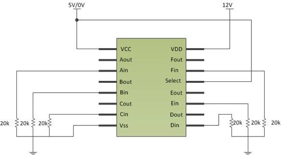
    I built test circuits as below schematic.

    When VCC is powered at 5V and VDD is powered at 12V, all output ports are at low when input ports are pulled down by 20kohm resistor. The Icc current is less than 1mA and Idd current is about 5mA.

    When VCC is powered at 0V and VDD is powered at 12V, all output ports are at low when input ports are pulled down by 20kohm resistor too. The Idd current is about 1mA.

    In the test, there is no high current and output switching when VCC=0.

    The logic forum engineers are experts and more familiar with the CD4504B. They will give your answers.

    Thanks

    Wei

  • There should not be any issues with Vcc at 0V and Vdd at 12V.  Be sure you inputs meet the rise and fall specs shon in the datasheet. If the inputs are too slow they can cause higher current ant the outputst to oscillate.

  • Yes my circuit looks like this (except for the Select input which is tied to ground).

    What is surprising is that initially everything is fine. I have to wait something like 1.5 to 2 minutes until the problem occurs (power consumption of board going from 1 uA to 8 mA ! 8000 times higher !!!).

    Then I discovered that if I power up the 5V for a short time, the circuit is back to the micro-amp range.

    Really puzzling!

  • Is VCC tied directly to Vss?

  • No. In fact Vcc comes from an LT3508 switching regulator, which is normally powered from Vdd.

    In deep sleep mode, there is a MOSFET switch that cuts off the Vdd input to the regulator, which in turn stops delivering the Vcc. There are some decoupling caps on Vcc, but I think that after more than 1 minute (when the problem occurs), they must be really empty!! 

    Measurement on Vcc show a little noise (in the millivolt range).

  • Vcc when shut off  it should be at 0V and not floated. The ESD/clamp protection diodes in the low side are tied to Vcc and  should not be floated. Also the switching threshold gets its reference form VCC and Vdd.

    You might try connecting Vcc to gnd when it is turned off ans see if that prevents the higher current that occurs after the part sits for a while.

  • Well I've tried to manually shunt Vcc and gnd when in deep sleep mode to make sure the Vcc is exactly zero... but the problem still happens.

    What I observe is that :

    - before the high consumption, all outputs of the CD4504B are low = 0V

    - when the high consumption occurs, I see that the outputs swing from a few mV to 40 mV...

    - when I keep my voltmeter probe on an output, its voltage usually decreases to a few mV, when I switch and probe another output, then I see the same kind of behavior, which tends to indicate that the voltmeter internal resistance has an impact on the measurement... But it is not systematic, and sometimes I see voltage rising, then falling back. Behavior is really chaotic.

    The high consumption may come from the 4043B latch that is behind the CD4504B, when it sees non-null inputs.

    The question is: why are the outputs of the CD4504B not at 0V ???

    Vcc is now exactly 0V, inputs are all tied to GND through pull-downs, only Vdd is present...

  • Can I see the schematic?   I am curious to see what the inputs are connected to. are they floating

  • The failing component is the first CD4504B

  • Any feedback on the schematics?

    Thanks!

  • Hello Chris,

    in the forum is written, that this posting is answered.

    ( header of posting was "CD4504B not working when Vcc = 0V ??"  )

    But i cannot find the answer. So what was the result of your analysis.

    best regards, peter

  • If you look at figure 11 in the datasheet it shows valid operating ranges.  I know the chart is horrible but you can see that neither voltage should go dow to 0V. 

  • Thanks for your fast response. I had a look to the figure 11, it shows, that at least 3V must be applied to VCC and VDD. But what does the sentence mean in the datasheet "Independence of Power-Supply Sequence" ??

  • I am not sure what that means. Usually a statement like this will mean that it does not matter what order the power supplies come up at.  Some translator require a certain power sequence.

  • Yes, but as you mentioned before, VCC may not be at 0V when a supply is conneceted to VCC nor vice versa. So VCC & VDD must be supplied at the same time with at least 3V, refering to figure 11 and your explanations.

    I think the sentence in the datasheet is not correct, because it makes believing, VCC or VDD can be applied while VDD or VCC stays at 0V => and this is not correct => i hope you can confirm this. 

  • I agree with you that the statement should be remove because it does not even make sense. Iw ill submit it for the change.

    Power up sequence is usually to prevent current spikes that might occur if powered in the wrong order. for instance the control pins may be powered by Vcca so Vcca should come up first.  However this does not mean the part will function correctly. It will only function correctly when both Vcc's are up.

    I beleive the statement in this case was meant to say that it will not damage the part or cause other issues if the part is powered in any order but it will not be functional until both power rails have been powered..

  • Hello Chris,

    thank you for your support. I know now how to proceed, and from my side there are now more questions.

    best regards,

    Peter