Hello,
I previously asked a question about the SN74AHCT574 (http://e2e.ti.com/support/logic/f/151/t/349518.aspx).
We have an old design (5V design) that is as follows:
uP (5V) --> 3 to 8 decoder (Active Low output, 5V) -> CLK (Pin 11 of SN74AHCT574, 5V)
5V --> inverter (5V) --> OE_N (Pin 1 of SN74AHCT574, 5V)
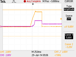
With the old design, all the outputs are low at power-up. Also, the OE_N follow the CLK Input signal (rise at the same time).
We created a new design (3.3V and 5V design) as follows:
uP (GPIO with internal pull-up of TMS320F28335,3.3V) --> Pull-up (3.3V) --> CLK (Pin 11 of SN74AHCT574, 5V)
5V --> inverter (5V) --> OE_N (Pin 1 of SN74AHCT574, 5V)
With the new design, some of the outputs go high temporarily at power-up. Also, the OE_N reaches 2V (Logic high level) several milliseconds before the CLK Input signal.
Oscilloscope outputs for both the new and old design are shown below (yellow trace is OE_N and pink trace is CLK).
In both designs, the SN74AHCT574 outputs are ONLY connected to the inputs of a ULN2803A.
Is there a way to correct the issue with outputs going high temporarily at power-up?
Another thing that I noticed is in the new design the SN74AHCT574 outputs are approximately 1V after reset (yellow trace is OE_N and pin trace is SN74AHCT574 output). What could be causing that issue?
Stephen
Old Design:
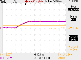
New Design:
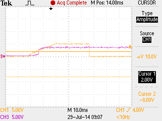
SN74AHCT574 outputs 1V after reset (New Design):