This thread has been locked.

If you have a related question, please click the "Ask a related question" button in the top right corner. The newly created question will be automatically linked to this question.

Output Level Error of LSF0204

Other Parts Discussed in Thread: LSF0204, SN74LV1T125

Hi...

My customer has designing LSF0204 for voltage translation.

But output level (B1, B2, B3) has occurred a problem such as dc offset (more than 0.5V) of output level.

So main system has stopped  due to MCU control problem. (Failure rate : 1/100, 1%)

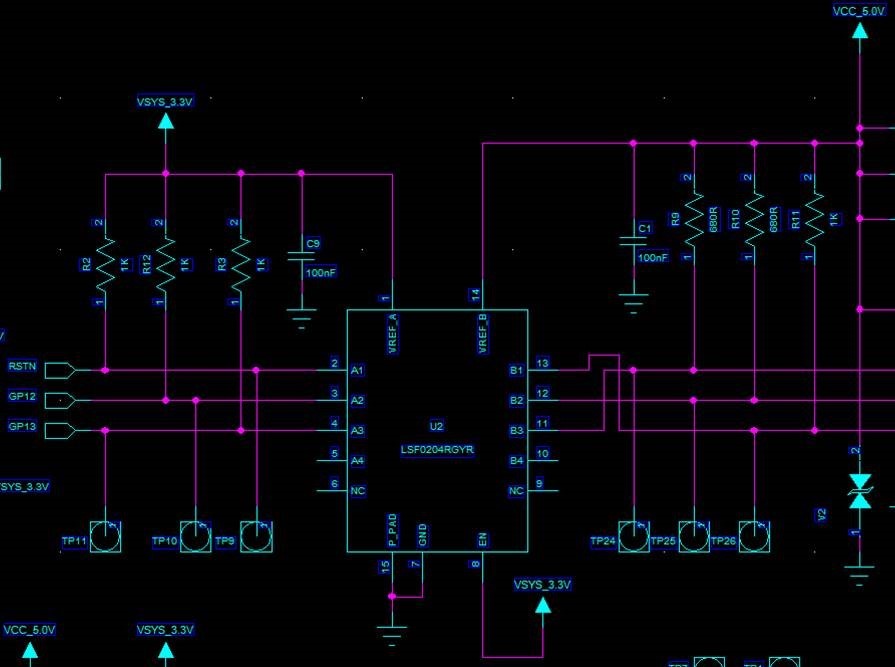
The schematic of my customer is as follows.

I need your advice for LSF0204 application.

Thank you.

  • JaePhil,

    Can you post scope shots showing the input/output waveforms, VREF_A , VREF_B, and GND?

  • Hi...Emrys

    I'm late for your response due to delay of my customer's response.

    The input and output waveform of LSF0204 are as follows.

    (Connection : UART Reset -> A1 -> B1 -> MCU, UART TX -> A2 -> B2-> MCU, UART RX -> A3 -> B3 -> MCU)

    1. The input waveform of LSF0204 (VREF_A=3.3V)

    a dc bias of low level is about 0.6V to 0.8V.

    2. The output waveform of LSF0204 (VREF_B=5V)

    a dc bias of low level is about 0.6V to 0.8V.

    if pull up resistor value of 5V is changed 680ohm to 1.5kohm, a dc bias of low level is changed 0.6V~0.8V to 0.45V.

    also a dc bias of input waveform is changed 0.6V~0.8V to 0.45V.

    My customer want to know why.

    3. Waveform with FT232 instead of LSF0204 (VCC=3.3V, UART TX Line)

    a dc bias of low level is about 0V. But a dc bias of UART RX is about 0.45V. My customer want to know why.

    We need your advice and help.

    Thanks.

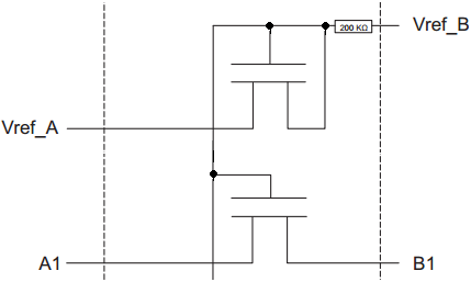
  • The LSF0204 is using a simple FET for translation.  This image shows the basic internal functionality:

    If the input voltage does not go to zero volts, then the output also will not go to zero volts.  I am unfamiliar with the FT232, but just based on the waveforms, I can tell you that it is a buffer style translator, using a standard logic buffer to translate between voltage levels.  Since the input is below that part's V_IL, the output is V_OL.  TI also makes many translators that work in a similar fashion if the customer would prefer that functionality (such as the SN74LV1T125).

  • Thanks for your response.
    I have several questions as follows.

    1. I think that low level of input and output waveform have effected by pull up resistor of VREF_B=5V and internal FET.
    Before internal FET turns on, input waveform is no problem and low level of input waveform is about 0V.
    I want to know why.

    2. Let me know the optimized value of pull up resistor of VREF=5V.
    Also I want to know that tuning of pull up resistor value has needed.

    Thanks.