This thread has been locked.

If you have a related question, please click the "Ask a related question" button in the top right corner. The newly created question will be automatically linked to this question.

74ABT16240 Behavior

Other Parts Discussed in Thread: SN74LV8151

Greetings:

I am investigating a problem for one of my customers.  I've distilled the symptom down to something that can be described in simple terms.  Here goes:

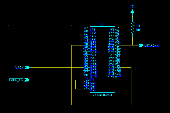
Picture a 74ABT1620 buffer.  One of the input channels receives a signal that has, at times, a slow rise time.  This is normal and acceptable.  The output enable signal that controls the buffer is clean and makes a nice, crisp transition to the buffer off state (OE/ goes high).  This occurs during the time that the input might be in an intermediate logic state, say 1.5V or something like that.  The output of this buffer has a 10K pullup, and drives a very short trace over to a CMOS input (low current/10ua).  What I am seeing is actual state transitions on the output for as long as 150ns after the OE/ is driven high.  The datasheet prop delay from OE/ high to tri-stated output doesn't support this.

My question is this - is it possible that the output is not going to a tri-state condition because the input is not at a hard logic level when the OE/ goes high?

  • Hi Carl ,

    The slow rise time of the inputs signal you mentioned in your post , how slow is it ? It is not recommended to have slow transition rate input signal into the device for its inherent issues . I have attached an app note talking about it .

    The OE going high should ignore the input levels and Hi-Z the part .What is "actual state transitions" are you observing ? any scope shots ?

    szza036b_interpretingLogic.pdf

  • Thanks Shreyas. Sorry for taking so long to reply.

    I would like to send you two files (1.schematic 2.scope capture). I cannot find a control/button that allows me to upload the files to you. My email address is metro.electronic@Verizon.net
    I will email the files to you if you will tell me how.

    The schematic and scope capture images will explain my question better. I will describe them here.

    Basically, the circuit is an input to the 74ABT16240, an enable for the 74ABT16240, and an output from the 74ABT16240. The input goes through one of the buffers. This first output is looped around to another input. The output on the scope trace is the output of the second buffer. The signals and colors are:

    Input - XACK/ - blue
    Enable - XACK_EN/ - magenta
    Output - LBXACK/ - yellow

    It appears to me that the 74ABT16240 is triggering on an intermediate voltage, thus causing the fast switching outputs. I need to understand this better.
  • You can send attach it here by using the "use rich formatting" option and selecting the insert file option .

    you may not see the actual attached file after selecting that but it will come through when you send it .

  •   Attaching files

  • Hi Carl,

    Thanks for sending over the schematics and scope shots .According to what you have described in the initial post  , i dont see that happening here exactly . The Yellow Y2 transition well before the OE goes high .

    Although , i want to point out couple of things here ,  

    There is a large undershoot on the OE and A signal of almost -2V which is violating the abs max conditions .

    The input transition rate on the A1 is extremely slow compared to the recommended datasheet spec of 10ns/V .There are also ringing on the A signal which probably translating to ringing on Y2 output which could be avoided by having smoother input signal.

    What about the unused input signals on the device ? I would suggest to gnd them if they are unused .It could result in unwanted behavior of the device .

    0755.slownfloatingCMOS_scba004c.pdf

  • Thanks for the quick reply Shreyas. Thanks for pointing out the undershoot. I'm not sure if this is due to my scope probe ground lead or not, but I will look more closely at this.

    Regarding the unused - they are actually tied to logic levels in the actual circuit, so no problem there.

    Regarding the slow fall time and slow rise time on the A1 input - my desire would be to eliminate the chatter on the output of the buffer due to the slow fall time and slow rise time. So this leads me to my actual questions.

    1. In an application such as this, is it true that ideally we would like to have inputs with edge transitions that are less than the switching speed of the 74ABT16240 ?
    2. Is there a device that is footprint compatible and contains Schmidt Trigger buffers?

    Thanks again Shreyas.

    Carl Reese
    214-794-4897 cell;
  • As a followup question - what is the danger (short term or long term) to the undershoot you pointed out in your response above?
  • Violating the abs max conditions doesn't kill the device in the short term since devices are robust enough to handle them . longer term reliability risk is definitely a concern to watch out for .Clamping the current to not go above the abs max condition would be advisable .
    There are no numbers on the duration of the violation before which the device damages .
  • There are many Hex Schmitt trigger devices i see in our portfolio but not one with 16bits . There is SN74LV8151 which is another ST option with 10bits .
    The ST will not have any input edge rate requirements but non-ST parts will have the input edge rate restrictions .