This thread has been locked.

If you have a related question, please click the "Ask a related question" button in the top right corner. The newly created question will be automatically linked to this question.

CD4504B input to Vdd internal diodes

Other Parts Discussed in Thread: CD4504B

1.  The input protection network shown in the datasheet for the CD4504B shows two diodes connected in series (anodes connected together) between the input and the Vdd supply.  What is the purpose of this instead of just an open circuit?
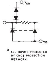
2.  If the Vdd supply is absent (due to supply failure perhaps) but the Vcc supply and the inputs are still present (15V), will the part be damaged? 

  • Hi Chris ,

    Good question . This looks to me as an error on the datasheet which is now being realized ! The inputs are protected by internal ESD diodes which needs to have anode to pin and cathode to Vcc ; so that whenever the inputs have voltages greater than Vcc , the protection diode limits the voltage by dropping across diode and thus protecting the internal circuitry .
    This can also be inferred from the abs max ratings table given on the datasheet which mentions the input voltage range to be -0.5 to Vcc+0.5V . (0.5V indicating the diode fwd drop ) .
  • Ok. Do you have any info on my question #2 in the original post?
    Thanks.
  • Hi Chris ,

    No damage to the device since diode is referenced to Vcc . Having no Vcc with inputs powered up would not be a good situation to have .