This thread has been locked.

If you have a related question, please click the "Ask a related question" button in the top right corner. The newly created question will be automatically linked to this question.

LSF0102

Other Parts Discussed in Thread: SN74LVC2G07, SN74LVC2G34

Hello,

I am looking to do a level translation between 3.3V (open drain) and 1.8V (push-pull)

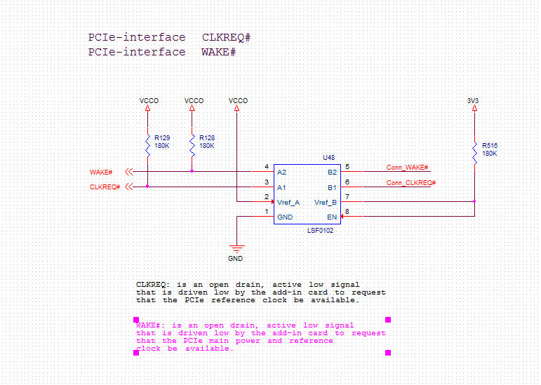
I am currently using the LFS102 successfully in a design, but I wanted to know if there was a part that you could recommend that would do the same function as the LSF102, but I don't require 3.3V to power the part. I wanted to remove a supply from my design and see if I could use this part to translate between a 1.8V -> 3.3V logic. As can be seen port B is an open drain with a pullup to 3.3V off of my PCB design. I would like to replace the 3V3 with 1V8 to remove the 3V3 power supply.

Is this possible with this part, or do you have another recommendation.

Regards,

Guy

  • Hi Guy Lemire ,

    VrefB is required to operate the part and bias the internal FET to control the device apart from being required for pullup . If unidirectional voltage is concerned , you can consider LV1T family of parts . It works with single supply with high to low or low to high active translation .
  • Hi Shreyas,

    I appreciate the response,but my question is if I can power VerefB and EN with a 1.8v supply instead of a 3.3V supply, but still have B1 and B2 operate with a 3.3V (off board) pullup. This will enable me to remove a 3.3V supply from this area on my PCB.

    regards,

    Guy

  • The recommended values of VrefB indicates that there needs to be 0.8V min difference w.r.t VrefA (VrefB >VrefA ) to operate .
  • Hi Shreyas,
    this parameter does appear to preclude me from using this part with lower voltages as I wished. Thank you for the response
  • Hi Guy ,

    I am sorry but the spec on the datasheet recommends to have that difference between Vrefa and B .
    I have tested some units in the lab with VrefA equaling VrefB and works alright , you could try in your setup to have VrefA and VrefB and use 3.3V pullup .
    In any case , if you are using the 3.3V and 1.8V on your board , will it not be easier to have it power up VrefB with it ?
  • Hi Shreyas,
    my reason for asking this is so that I can run both VrefA and VrefB off of a 1.8V rail and not need 3.3V. I am finding that the majority of my power supplies for my PCB designs are migrating to 2.5V and below, with many now at 1.2V-1.8V, so if i can remove a 3.3V supply that would help in my layout.

    The 3.3V pullup is located on another PCB through a PCIe edge connector.

    Regards,
    Guy
  • Hi Guy ,

    Since TI should bind by the datasheet , the recommended conditions needs to be followed .
    If you want to try with same Vref A and Vref B you can try but it may or may not work always and you should accept the reliability issues if any .
  • Hi Guy ,

    You can also consider some transceivers which will work with VccA and VccB being the same but the output cannot be pulled up using resistors . It kind of defeats the purpose of the transceivers actually.
  • Guy,

    Do you need bi-directional translation here (ie is data going from 1.8V to 3.3V side and vice-versa on the same channel?).  If the answer is 'no,' I would recommend looking at the LVxT family of translation parts.  You can do 1.8V -> 3.3V translation easily with SN74LV1T125

  • This does not defeat the purpose at all......I am translating from an open drain at 3.3V to a 1.8/1.5V IO, so I need a translator chip...the who idea gets back to my original question..using one supply (1.8V) to power the translator chip versus two (1.8V, 3.3V)

    regards,

    Guy

  • Guy,
    Please correct me if I'm wrong, but from what all I've read so far, it sounds like both lines are uni-directional translation from 3.3V (open-drain output) to 1.8V. This could be accomplished with a pull-up resistor to 1.8V on the open-drain line and no translation device between the two. Am I missing something?
  • Hi Emrys,
    both the CLKREQ# and WAKE# are by PCIe spec 3.3V open drain signals. the pullup resistor is usually on the root complex (mother board)

    Because I am using an fpga with 1.8V IOs, I cannot expose my fpga to a 3.3V signal. I need a bi directional translator because I have to both monitor and control each of the signals.

    Not sure I understand your comment about using a 1.8V pullup on the open drain..

    regards,
    Guy
  • Guy,

    Thanks for the clarification.  I believe I have a solution that will eliminate the need for a 3.3V supply on your card with the use of 2 parts.  Basically, an over-voltage tolerant input buffer will be used to read the 3.3V signal, while the line can be driven low by an open-drain output buffer - both of which operate at 1.8V.

    The SN74LVC2G07 can handle up to 6.5V on an output, regardless of Vcc, and contains 2 open-drain buffers.

    The SN74LVC2G34 can handle up to 6.5V on an input, regardles of Vcc, and contains 2 push-pull buffers.

    I have thought of a few ways to do the layout -- this is one option using separate 'monitor' and 'drive' lines.

    Sorry for the crude drawing -- please let me know if I can be of further assistance!

  • Hi Emrys,
    thank you for the reply. Please close this case.

    regards,
    Guy