This thread has been locked.

If you have a related question, please click the "Ask a related question" button in the top right corner. The newly created question will be automatically linked to this question.

regarding current consumption issue of SN74LVC4245ADWR level translator

Hi team

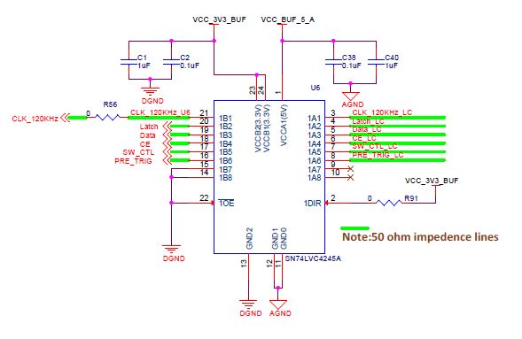
currently , i am using SN74LVC4245ADWR level translator in my custom design. we are converting 3.3V loigc level to 5V logic level and vice versa(5V to 3.3V).

when conversion is 3.3V to 5V logic level, current consumed by level translator is approximately 10 mA, but when conversion is from 5V to 3.3V logic level, current consumed by level translator is approximately 110mA. Is it ok fort his level translator. if yes then then please suggest some other level translator which wlil consume less current during 5v to 3.3V logic conversion. 

I am attaching my reference design snapshot. Please help me to get rid of this issue. in the design input side is BUS A and output side is BUS B.

  • Hello Chandan,

    Drive current can be as high as 24mA per IO channel, so current can exceed 100mA if that is what is required to drive your output. Are you sure the output being driven is not causing this high consumption?
  • we are not driving any circuit using these control signals. we want to give these control signals to FPGA GPIO for further processing.
    Actually our requirement is to give receive control signals at 5v Logic level and to give these control signals to FPGA GPIO. But FPGA GPIO can accept input at 3.3V LVCMOS logic level. Can you suggest some other alternative method for doing this process. Our main aim is to reduce the current consumption of our design.
  • Hi Chandan ,

    Couple of things on the circuit:
    1) Your direction pin is held at 3.3V but they are referenced to VccA voltage . this will increase the Icc current from the device ; look for delta Icc .This will most likely be your major source of static current consumption. Please have it tied to VccA.
    2) with DIR high , the A ports are inputs and B are outputs and you have 1A7 and 1A8 open . Look for slow and floating inputs app note attached here . you will have to ground those instead of B pins.


    The hope is that your FPGA control pins are high impedance inputs not loading the LVCC4245A device .