This thread has been locked.

If you have a related question, please click the "Ask a related question" button in the top right corner. The newly created question will be automatically linked to this question.

Level Shifter for RMII Bus

Other Parts Discussed in Thread: TXB0108, SN74AVC16T245, TXS0102, SN74AVC16T245-Q1

Hi everyone,

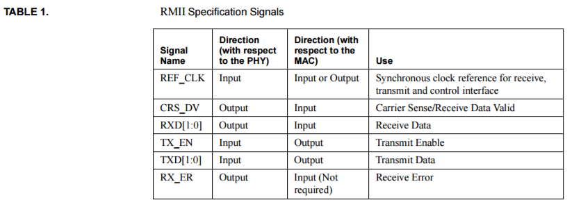
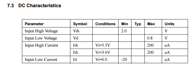
I need a level shifter for a RMII bus. Bus contains one 50 MHz clock, and data signals that are synced with 50 MHz clock. Voltage of PHY side is 1.8V and voltage of user side is 1.5V or 3.3V. I can configure user sides voltage but i prefer 1.5V. I can use one of TXS0108, TXB0108 or SN74AVC16T245. Can i use one of them or do i need to look another shifter?

  • I would recommend the AVC16T245. According to the RII specification, current draw can be as high as 200uA but the TXS and TXB translators can only provide up to 20uA of current when driving a logic high or low. The AVC16T245 can provide several mA of drive current and can meet the required clock frequency of 50MHz.
  • As far as I know, RMII uses five unidirectional signals in one direction, three signals in the other direction, and one bidirectional signal (MDIO). Is this correct?

    The SN74AVC16T245 requires that one direction is chosen for each group of eight bits, so it looks as if it is not possible to handle MDIO with it.
    If it is not possible for your microcontroller to set the MDIO direction manually, you need a level shifter with automatic direction sensing, i.e., a TXB/TXS device. (The automatic direction sensing requires that the signal can be driven with at least 2 mA.)
  • I think you are correct, there actually is a bidirectional signal. I was referring to this RMII Specification document. On page 4, the specification calls for 8 unidirectional signals but this does not include the bidirectional management signal. 

    If the bidirectional MDIO line is included then the SN74AVC16T245 will not work. Would you be willing to use a solution that required more than one translator? I am hesitant to recommend an auto-direction translator due to this 200uA input high current spec, which will reduce the VOH of TXS and TXB translators. 

  • Well, strictly speaking, using 1.8 V or 1.5 V is not covered by the RMII specification anyway. It's likely that for these devices (whatever they are), the actual input current is much lower than 200 µA.

  • RMII bus of device contains signals that listed below:

    RMII_REFCLK Input    Reference Clock input

    RMII_TXD0     Output Transmit Data output 0

    RMII_TXD1     Output Transmit Data output 1

    RMII_TXEN     Output Transmit Enable output

    RMII_CRSDV  Input     Carrier Sense/Receive Data Valid input

    RMII_RXD0     Input     Receive Data input 0

    RMII_RXD1     Input     Receive Data input 1

    And a MDIO interface for configuration. I will use TXS0102 for level shifting of MDIO. Data part of bus is bi-directional.

    I can use SN74AVC16T245 or its qualified version SN74AVC16T245-Q1 for RMII bus. These level shifters main purpose is asynchronous communication.

    From SN74AVC16T245-Q1 data sheet:

    "The SN74AVC16T245-Q1 is designed for asynchronous communication between data buses."

    Also buffer can achieve 380 Mbps from 1.8V to 3.3V (150 Mbps for 1.5V), and it seems that device can level shift RMII bus. But my concern is propagation delay. Period of RMII bus is 20 ns and maximum propagation delay of level shifter is 

    tPLH 8.2 ns, tPHL is 8.2 ns => total 16.4 ns for 1.5V conversion. (VCCA is 1.5V)

    tPLH 7.4 ns, tPHL is 7.4 ns => total 14.8 ns for 3.3V conversion.(VCCA is 3.3V)

    Delays of all level shifters I/O's will not be same. Do these delay values be a problem for RMII bus?

  • Understanding and Interpreting Standard-Logic Data Sheets (SZZA036) says in the tpd entry:

    A common misconception about logic devices is that the maximum data-signaling rate (or maximum frequency, as it is commonly misnamed) is equal to the inverse of the propagation delay. The maximum data rate on buffers is dependent on several factors, such as propagation delay matching, input sensitivity, and output edge rates. A device can have a high maximum signaling rate if the propagation delays from low-to-high and high-to-low are matched, the input is fast enough to respond to the fast data rate, and the output edge rate does not interfere with the low and high-level steady states.

    You'd have to look at the skew parameters (if they are specified). Anyway, "380 Mbps" means "380 Mbps".

  • Hello,

    You should not have a problem. I think you should refer to the answer in this thread for more information about tPLH and tPHL vs data rate:

    e2e.ti.com/.../514181

  • Thank you for answers and help.