This thread has been locked.

If you have a related question, please click the "Ask a related question" button in the top right corner. The newly created question will be automatically linked to this question.

[SN74LVC1G125-Q1] Please Review the SCH and Operation

Other Parts Discussed in Thread: SN74LVC1G125-Q1

Hi Team,

Please review the SCH as attached.

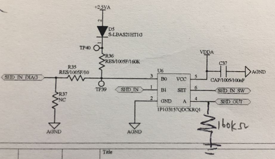
I have one question.

The Vcc =5V, SET is 0V / 5V. A = 5V to 5.3V

SET=0V, B0 is turn-on at A=5V

SET=5V B1 is turon-on at A=5V. but A is changed to 5.2V then B0 is also is floating is 2V. Is this correct?

in D/S, A is max 5.5V. 

Best Regards,

Nate

  • Nate,

    This thread has been moved to the Logic forum for more appropriate support.

    Regards,
  • When SET is high, B0 is not floating but at the voltage imposed by the pull-up resistor R36 and the diode. The voltage drop over the diode depends on the current through it, which depends on the load on SHD_IN_DIAG.
  • Hi Nate,

    I noticed that your question is about SN74LVC1G125-Q1, a buffer, but your schematic shows a 1:2 analog switch.  Can you clarify?

    I have redrawn your schematic to more clearly show what's going on:

    Can you tell me what is at each highlighted box?  From the sounds of it, there is likely a small current passing through the diode which, as Clemens said, is biasing the B0 port to ~2V (which is what you would expect if the diode were turned on, even slightly - that's a standard silicon diode with minimum forward voltage around 0.4V)

    As for the voltages - you are correct that you can apply up to 5.5V to the device -- if A goes up to 5.3V, that is no problem.