This thread has been locked.

If you have a related question, please click the "Ask a related question" button in the top right corner. The newly created question will be automatically linked to this question.

SN74GTL2014: TI GTL2014 design doubt

Part Number: SN74GTL2014

Dear Team,

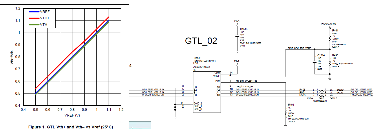
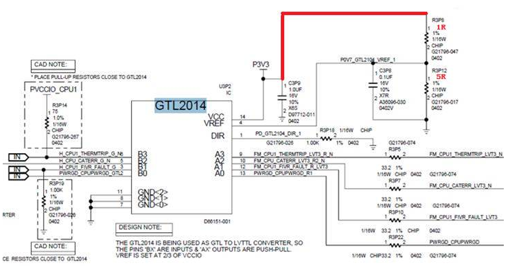
There is a design doubt about GTL2014. According to TI’s reference design, Vref is using PVCCIO which the PWR bring up after P3V3, thus we would like to change PWR doamin to P3V3 making GTL2014 operated at same time when P3V3 bring up, does TI identify this design?

Thanks!

  • Hi Jim ,

    could you confirm your question again ? are you referring to the power sequencing for GTL2014 ? which reference design document are you referring to ?
  • Hi Shreyas,

    Please see the attached photo as below.

    On customer board, P3V3 is valid before PVCCIO_CPU0 (power domain of B0/B1/B2/B3).  During the period that P3V3 is valid butPVCCIO_CPU0 is not ready yet, they found B0~B3 signals and VREF voltage levels are very close around 0.xxV.  They're afraid that B0~B3 voltage level would be within the range between RED and BLUE lines as below which could cause unstability of A0~A3 output voltage levels.  Therefore, they're asking if they can change VREF to P3V3 domain which is the same domain as Vcc pin, to make sure B0B3 will always be lower than Vth-.  (VREF-0.75V and B0~B3 is 0.xxV.)

    May I know what is your comment?

    Thanks!

  • Hi Antony,

    As a disclaimer, this reference design was created by Intel, so I'm just giving you my opinion here.

    I believe that the VREF pin is connected to a voltage divider from the CPU's operating voltage because this pin controls the high/low threshold of the CPU's communication lines. If the threshold is controlled via P3V3, it is possible for the CPU voltage to change and the threshold to remain constant, resulting in data loss.

    Assuming that the customer is confident in the correct VREF voltage, the suggested solution sounds viable to me. I just wouldn't want to go against the reference design.
  • Hi,

    Considering the behavior of our chip only, do we have any sequence requirment between VCC and VREF? Can VCC and VREF turned on at the same time?

    Thanks!

    Antony

  • The VREF pin's recommended maximum is VCC/2 -- therefore it would violate the specs to turn on VREF prior to VCC.

    I would recommend powering VCC first, then VREF, however turning them on at the same time is fine so long as they maintain the requirement of VREF < VCC/2