Part Number: SN74125
I am using SN74LVC1G125 in my design. The OE# pin of the buffer is driven using a clock pulse and the input Pin A is always at 0 (grounded). The output Y has a pull-up resistor of 10K. Hence when the frequency of the clock pulse driving OE# signal is more than 200KHz, the output Y is always zero. Let us know the reason for this. Whether the OE# will not work beyond 200KHz and let us know the frequency characteristic of this IC with respect to OE# input
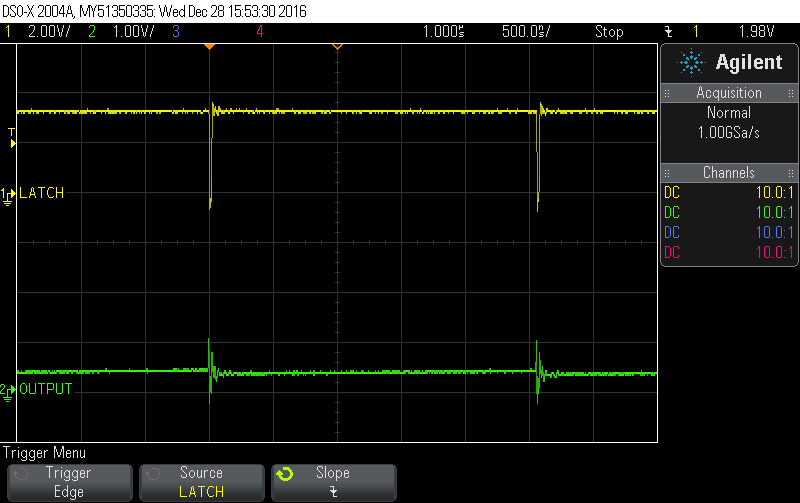
DATA_LATCH signal is driven by a 400KHz clock pulse. And the Output Y is always zero in the below circuit