This thread has been locked.

If you have a related question, please click the "Ask a related question" button in the top right corner. The newly created question will be automatically linked to this question.

SN74AVC4T245: Always getting 0V at Port A side of SN74AVC4T245

Part Number: SN74AVC4T245
Other Parts Discussed in Thread: SN74LVC125A, SN74AVCH4T245

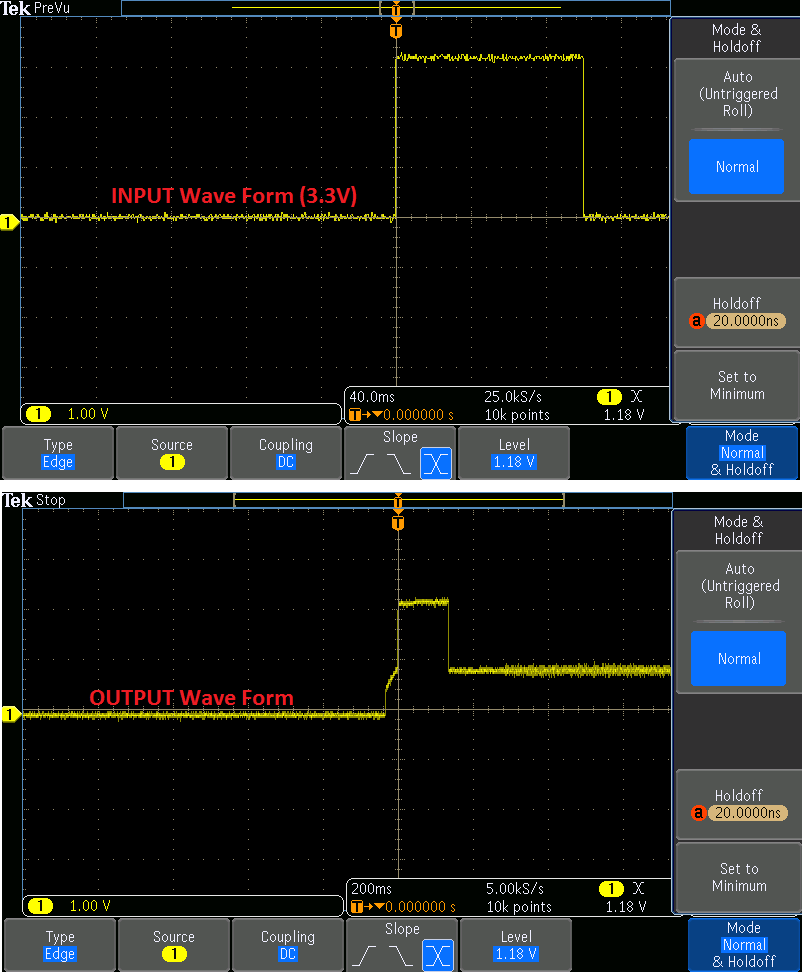
Hi....I'm using SN74AVC4T245 in my design. This "SN74AVC4T245" used to translate 3.3V to 2.8V as mentioned in the below schematic. I didn't connect any pull-up resistors on A or B port bus. 

I'm always getting 0V at Port A (output port) even-though If I drive high at B Port (input port). Do you have any idea for this issue ?

Regards,

Azlum

  • I see no obvious mistake in the schematic.

    Are both supply voltages actually there?

    Are the A outputs actively driven by the translator, or high impedance (check with a pull-up resistor)?

    (For unidirectional down-translation like this, a 2.8-V buffer with 3.3-V-tolerant inputs like the SN74LVC125A would be somewhat simpler to use, and be cheaper.)

  • Both 2.8V and 3.3V are present. I have connected 10K pull up resistor at port A (between 1A1 and 2.8V). Still port A driving 0V.
    Do you have same foot print part with internal pull-up ?
  • If port A is actively driven, all power supplies and the OE and DIR signals must be OK.

    In theory, the only remaining possible source might be the B signals. Are they valid (and not floating)?

    There is no such device with internal pull-ups. (The SN74AVCH4T245 has bus-hold circuits, but I guess a random state is not useful.) If there are times when there is no valid signal, you must use external pull-ups.

  • Hello Mohammed,

    Your schematic looks fine, you should be getting an output at A port. Unfortunately we do not have a part with the same foot print with internal pullups. The closest thing we have is the TXS0104 which has 10k internal pullups but has a slightly different footprint.

    With the pullup attached to the A port you are still seeing 0V which makes me think there may be a short to GND somewhere. Are you sure the device you have connected to the A port is not somehow pulling the signal to GND? Have you tried removing the peripheral at the A port and testing to see if you get any output with the pins at A port left open?

  • Hi....

    I have observed one more unexpected behaviour. I have driven high at input port (Port B). But the response at output port is not as expected. I'm getting 2.2V high instead of 2.8V.

    Please find below CRO waveform (input vs output).

    Regards,

    Azlum

  • Hello Azlum,

    Again, I have to ask. Have you tried removing the peripheral at the A port and testing to see what your output looks like with the A port left open?
  • Hi..I tried by isolating the load. I didn't connect any load at port A. 

  • What is the result? Do you get 0V at A port with no load or do you get the glitch from the screen shot posted above?
  • I'm getting the wave form like above screenshot. No matter load is connected or not. Always the same wave form input vs output waveform.

  • Hello Azlum,

    Can you try a DC test? Apply DC 0V to the input and capture the output. Then, apply a DC 3.3V to the input and capture the output.

    Also, can you get another capture of the above scope shot with the input and output captured on the same timescale? Right now, the input is a 40ms/div and the output is at 200ms/div, making it hard to compare the two.