This thread has been locked.

If you have a related question, please click the "Ask a related question" button in the top right corner. The newly created question will be automatically linked to this question.

LSF0108-Q1: LSF0108-Q1

Part Number: LSF0108-Q1

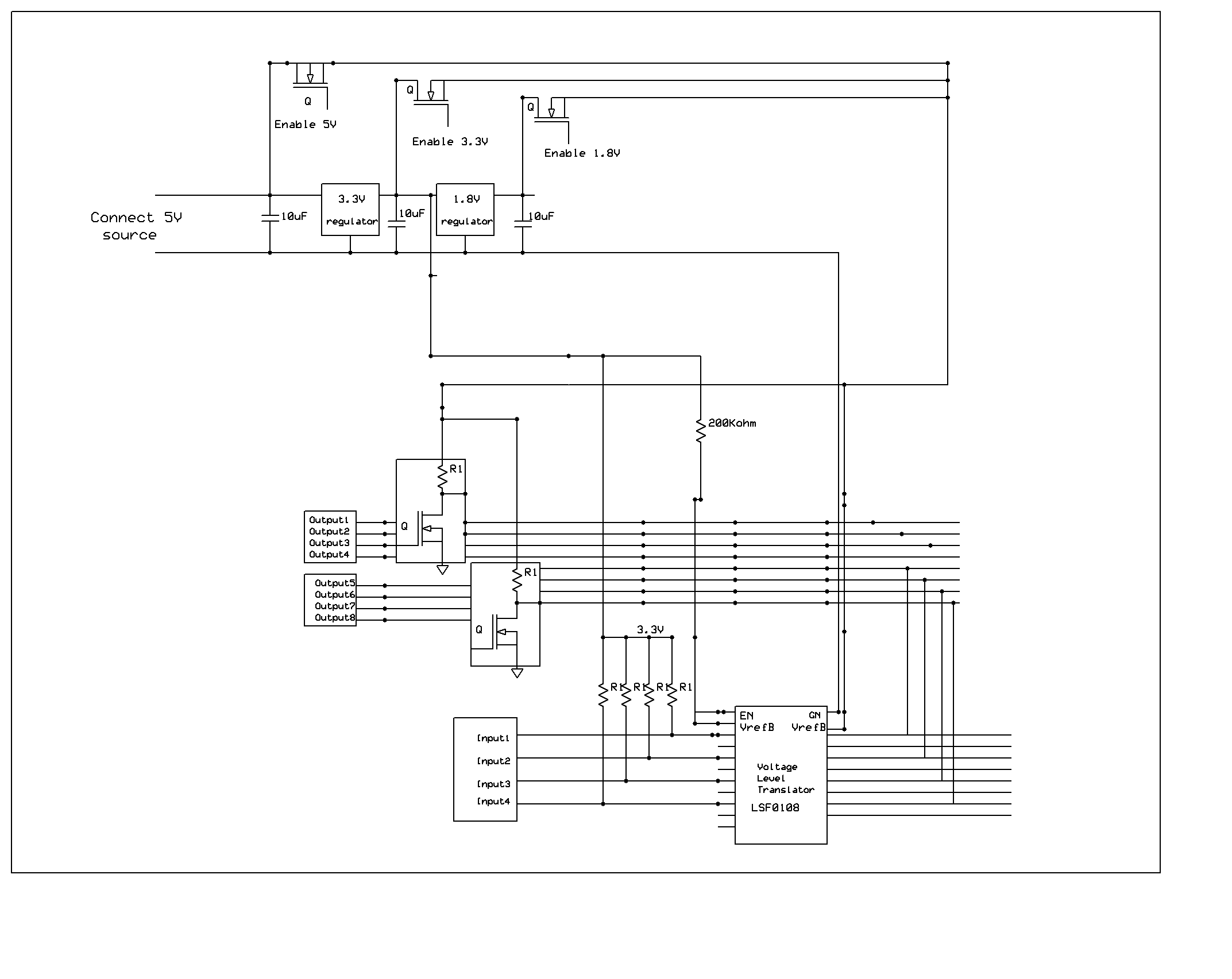
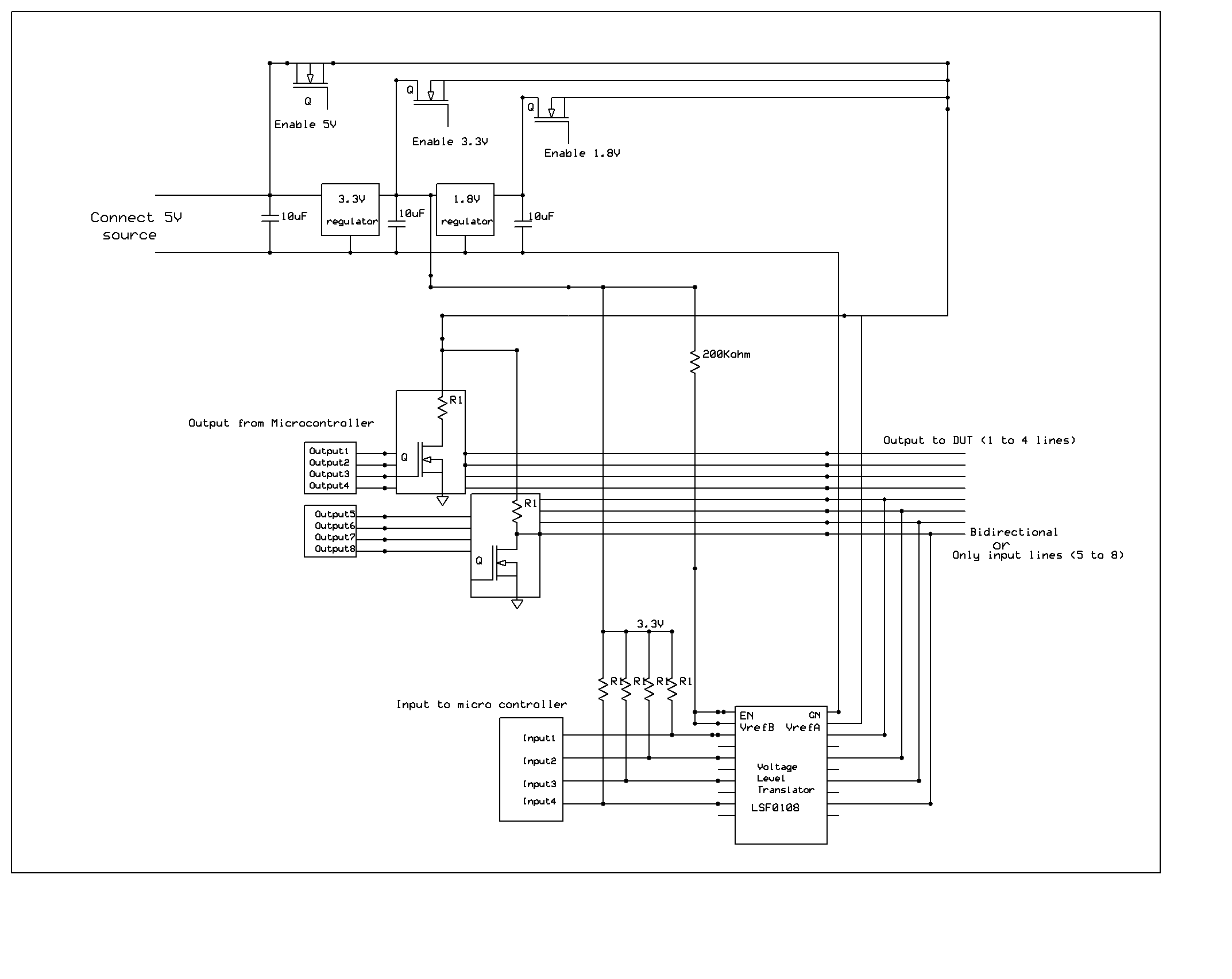
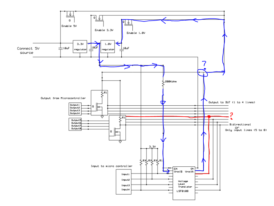
My output is not reaching zero. Even the input is not g etting to zero when I turn on the voltage translator. Red waveform is input and yellow one is output. Offset in input is due to voltage translator only

  • Hi Chaitanya,

    The LSF series of translators are passive in nature and will not redrive a signal. If you need your output to be lower than your input, you will have to switch to an active translator.

    It's likely that the reason your input is not making it closer to zero is because your driving device cannot sink very much current. Note that current from the pull-up resistors on _both_ sides of the LSF will sink into the driving device.

    If you can post a schematic of your system we might be able to help.
  • I am trying to implement bidirectional functionality using the above schematic diagram. The voltage regulators are to select the output voltage level. I always want to sense the input at the output lines 5,6,7,8 through voltage level translator. And I want the 3.3V always at the input side i.e at Vref A. While on B side I will be giving the inputs at 1.8, 3.3 and 5V  pulses. 

  • I also have another doubt, For the voltage translator the input should be zero and High-Z or Zero and one.
    Secondly In the above schematic when I am giving input to voltage translator from the output pins at Vref B I am getting the output at Vref A side. But when I am Disabling the outputs shown in the schematic and trying to give input to voltage translator on Vref B side through function generator I am not getting the output at Vref A side. And the output is floating in Air
  • I see several problems with this implementation.

    First, you r schematic has both VrefA and B labelled as VrefB -- VrefB must be tied to EN and then connected through a 200kohm resistor to a voltage at least 0.8V higher than the voltage on VrefA.

    VrefA will be sourcing current - something which most LDO regulators would not like (they are designed to source, not sink, current).

    I think the fix for your system is to use the circuit I showed in this thread.

    Since that circuit only relies on a single constant supply (3.3V), then you can change your output to 5V, 3.3V, and 1.8V without any issues.  Note that you must have pull-up resistors on _both sides_ of the LSF device for this to work.

  • Hi I have tried by connecting the circuit which you have said But I am getting the same. I am giving input [3.3V - Square wave] to that from a function generator. But getting the output as constant at low value of pull up resistor value. And for high value of pull up resistor It is not reaching to High logic level(3.3V). I think that might be because when the function generator is giving zero it is not sinking the current. But Will it be the same even with the micro controller ( Will It ground the pin while giving zero as input to translator or not )

  • I am giving zero to mosfet from output line 5, So that the switch will be open. Now what I am doing is by enabling the 5V voltage at Vref A pull up I am giving input through a function generator at the Bidirectional pin 5 I am trying to see the output at input pin 1 (Using CRO) But the output is not reaching zero in case of small pull up resistor  and is not reaching 3.3 when I am using large pull up resistor. 

    But When I am giving the input at Output pin 5 using function generator enabling 5V pull up I am able to see the same input which I am giving at output pin 5 at Input pin 1.

  • I'm a bit confused by your schematic.

    I highlighted two paths here.  The red is the A-side communication line where there should be a pull-up to VCCA, and the blue path shows the current path for the bias circuit (and why the LDO regulators won't work in this situation).

  • you have drawn a red line that is the input line and the pullup in the mosfet block( The mosfet will be open) acts as pullup on A side. And the blue line which you have drawn is the ref voltage for A and B side. On B side the reference is always 3.3 and on A side it will change depending on the 3.3V, 1.8V or 5V switch in on state. I am giving input pulse near the question mark line

  • You definitely can't have VrefA at 5V and VccB at 3.3V -- the translator won't work that way.

    Perhaps you should step back and simplify your circuit first -- just get the translator working with none of the other stuff (5V to 3.3V perhaps). Many times I find this to be a good way to approach a circuit that's giving me problems.
  • But when I am connecting the circuit as above I am getting the output ( if the source is able to sink current) . I have replaced that ref with 1Mohm and 267kohm with 3.3V ref on both sides (which was suggested by you in first post).

  • But In data sheet they have given a example for multiple voltage level translation. Where they give ref at on volt and pullup at other voltages. Similarly my initial design was like maintaining VrefA at 1.8 volts but pullups might be at 1.8 or 3.3 or 5V. And VrefB always at 3.3V and pullups will be at 3.3 V . But when I connected like that I was getting problem. Later I gave same ref voltage at A as pullups It started to work. How is it possible giving refVA =5V and pullups voltage 5V it is working
  • I also don't want bidirectional communication. I want the input at REF A side to reach Ref B side i.e 1.8 or 3.3 or 5V to 3.3V