This thread has been locked.

If you have a related question, please click the "Ask a related question" button in the top right corner. The newly created question will be automatically linked to this question.

SN74AVC32T245: Output impedance, DOC circuit

Guru 20090 points
Part Number: SN74AVC32T245
Other Parts Discussed in Thread: SN74AVC16T245

Hello,

I have the question about the output impedance of SN74AVC32T245.

Could you please let me know the output impedance when we use Vcc=3V, Ioh=12mA at high impedance state?
Also please let me know the variation of output impedance.

According to application note of SCEA009B, the output impedance is calculated with (VOH - Vcc)/IOH or VOL/IOL.
If I calculate with Vcc = 3 V and Ioh = 12 mA, I think the output impedance will be below.
(3 - 2.3) / (-12 mA) = 58.3Ω and 0.7/12mA = 58.3Ω
Is this calculation for high impedance correct?

According to Figure 5 of SCEA009b, there is a period of Low Impedance mode for the fast slew rate and it returns to High Impedance mode in the last stage.
Is this behavior same with SN74AVC32T245?
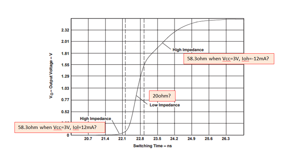


Best Regards,
Ryuji

  • All AVC devices have DOC.

    You can derive the output impedance from the slope of the curves in figures 1 and 2. Anyway, the description of figure 5 and FAQ 7 list them:

    In the high state, the output RON varies from approximately 50 Ω in the high-impedance mode to approximately 30 Ω in the low-impedance mode. In the low state, the output RON varies from approximately 50 Ω in the high-impedance mode to approximately 20 Ω in the low-impedance mode.

    But why do you want to know the exact value of the output impedance? Usually, what matters is how much current you have to charge the capcitance of the load.

  • Hello Ryuji-san,

    I have also sent an email with some additional details to your local TI contact, but I wanted to comment here as well. The output impedance of a logic device isn't constant while the output changes from low to high. You can look at it as a single pFET connected from Vcc (source) to the output (drain), and the gate tied to 0 V (for the sake of HIGH logic level output impedance calculations).

    Your equation is correct, and what you show on the graph looks to be correct as well, however the calculation of 58.3 ohms doesn't give you the output impedance during the transient -- it gives you the maximum output impedance in the DC output state.

    Unfortunately, we cannot guarantee a specific output impedance for all devices - this will likely change some from one lot to another, however you can be certain that the maximum you calculated will not be exceeded.

    Can you tell us why you need this value? Typically impedance matching with logic is not necessary, and if we know more we might be able to help.
  • Hello Emrys san,

    Thank you for your support.

    They use this device for above 60MHz of clock signal.
    There is the possibility of decreased the signal integrity if the output imepedance is varied.
    They couldn't use termination/dumping resistor due to mounting aria is limited.
    When they simlated with low output impedance of 20ohm, overshoot and undersoot was occured over1V.
    In this case the receiver absolute maximum ratings may be violated.

    Thus, they need this information.

    Best Regards,
    Ryuji
  • The DOC circuit does not use the low impedance when the output is near GND or VCC, to prevent ringing.

    Did that simulation include the DOC circuit?
    Did you test with an actual device?
  • Hello Clemens,

    DOC circuit is note included in the simulation.
    They will test the SN74AVC16T245.
    Since the SN74AVC32T245 is BGA package only, we will test the SN74AVC16T245 TSSOP.

    Best Regards,
    Ryuji