This thread has been locked.

If you have a related question, please click the "Ask a related question" button in the top right corner. The newly created question will be automatically linked to this question.

TXS0102: Problems with TXS0102 level shifter

Part Number: TXS0102
Other Parts Discussed in Thread: TXB0102

Hi

I hope that some of you can help me.

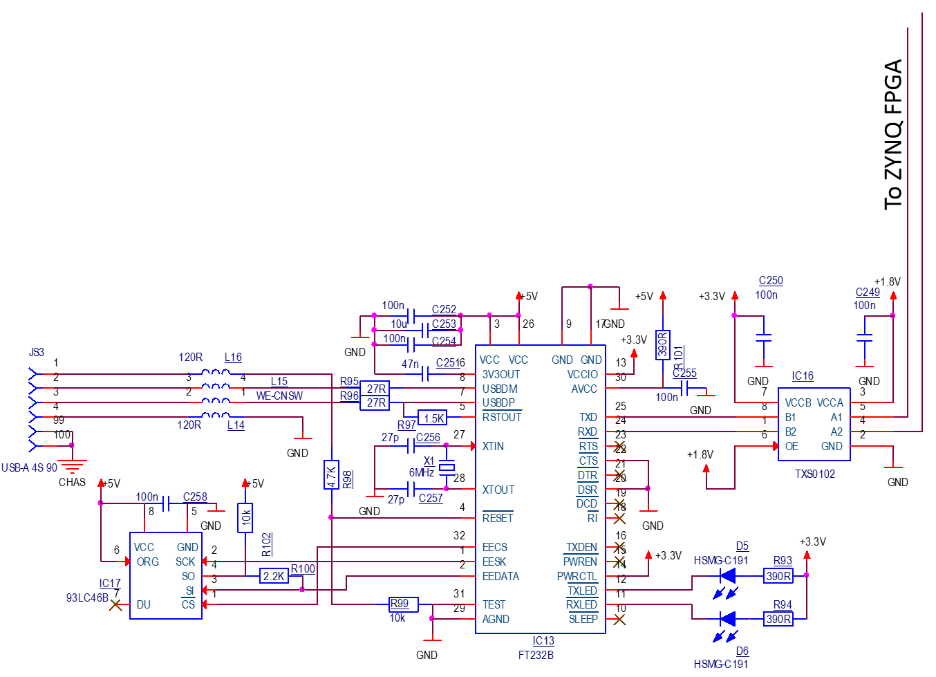
I have used the TXS0102 to level shift the TXD and RXD between a 1.8V FPGA and 3.3V UART/USB (FT232B).

The problem is that it does not work!

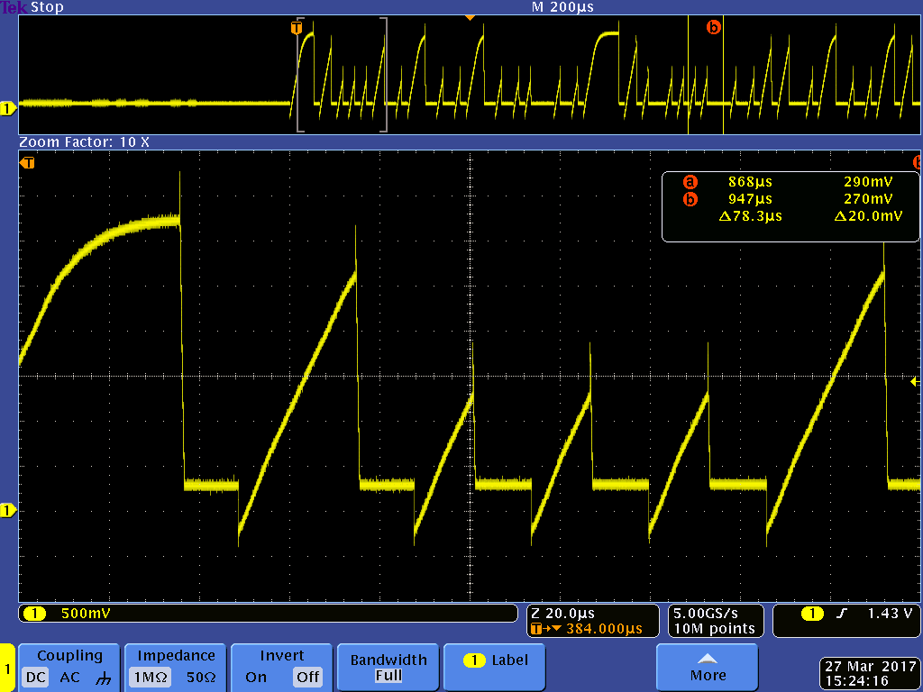
Sending data from the FPGA to the USB, just gives rubbish data on the USB.

The signal (RXD) from the FPGA to the TXS0102 looks ok

But the signal from TXS0102 to FT232B looks strange:

I will try to put a 1Kohm pull-up to the FT232-TXS0102 signal and hopefully that will produce the correct output.

I have two questions:

  1. It looks like the TXS0102 is inverting the signal. Is it supposed to do so?, or if not: What could be wrong?
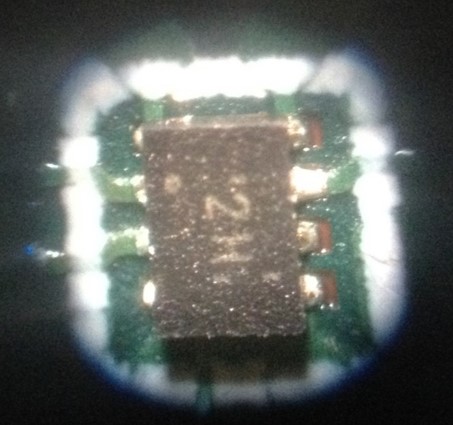
  2. It is difficult to see if the IC is mounted correctly. Maybe the PCB supplier has turned it 180 degrees. When looking at the picture, pin 1 is supposed to be in  the upper left corner. Can you confirm that it is positioned correct?


Best regards

Søren

  • What is the drive strength of the FPGA? Are all grounds connected correctly?
  • As far as I can tell and measure, all GND are connected correctly.
    We are using a XILINX ZYNQ as a FPGA. The drive strength is programmable and can be switched between 4, 8, 12, 16 and 24 mA.
    I think it is set to default (12mA)
  • Hello Søren,

    How long are the traces between the TXS0102 and the FT232B? Have you tried a simple DC test? Could you try to apply a 1.8V DC signal to the input at see if it drives high at the output and apply a 0V DC signal to the input and see if it drives low at the output?

    It looks like the package is oriented correctly.

  • The traces are approx. 10 to 15mm.

    We have not tried a simple DC test (mainly because it would be very difficult to apply a signal to the 1.8V side. (all traced is inside the PCB)).

    We have now tried to remove the TXS0102 and then we have a nice 1.8V signal from the FPGA.

    We will probably end up discarding  the TXS0102 and find another solution :-(

  • Perhaps the TXB0102 would be a better solution as it is designed for push-pull I/O. It is pin-for-pin compatible with the TXS0102..
  • Thank you for your inputs.

    The reason for problem has been identified.

    The schematics was made for the DCT/DCU package, but when we did the PCB layout, we decided to use the DQE package.

    For some reason, pin numbers and functions are not the same for these different packages.