This thread has been locked.

If you have a related question, please click the "Ask a related question" button in the top right corner. The newly created question will be automatically linked to this question.

SN74AUP1G74: USING POWER-ON AS TACT SWITCH

Part Number: SN74AUP1G74
Other Parts Discussed in Thread: SN74AUP1G17, , SN74LVC1G3157, SN74AUP1G14, SN74AUP2G17

Hello,


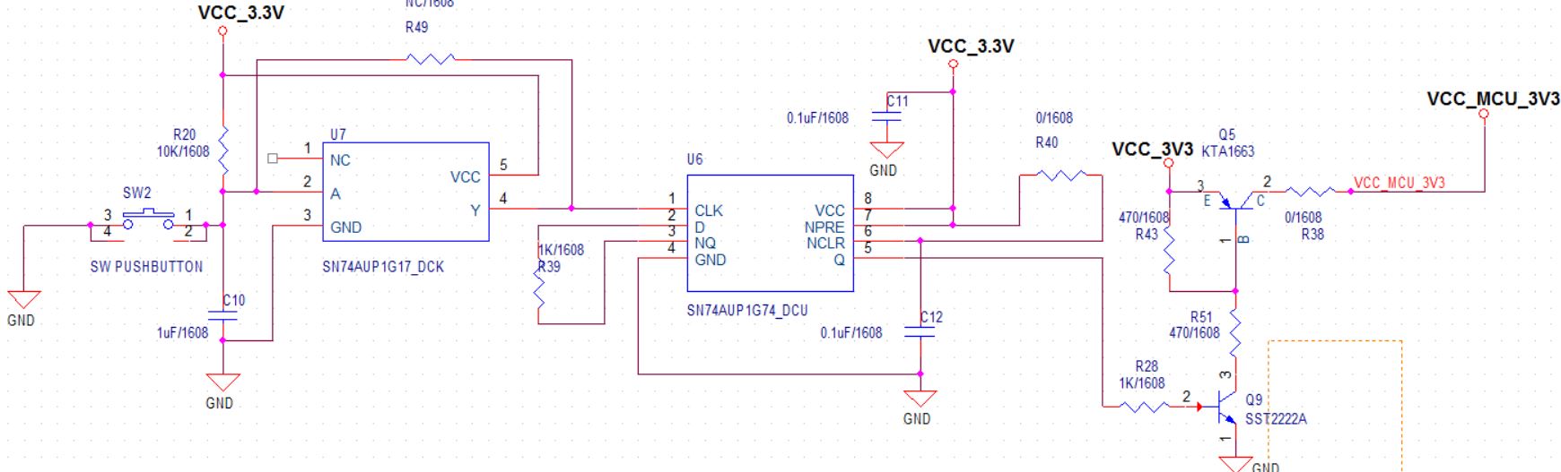
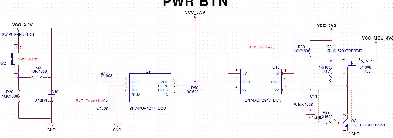
I want to use power-on as tact switch, so draw SN74AUP1G17(BUFFER) and SN74AUP1G74(FLIP FLOP) seeing datasheet.


I wonder this circuit maintaned(power-on)  Q=H ,  confirm this circuit is right.


Thank you, sir

  • please reply ASAP , Thank you, sir
  • This looks somewhat similar to figure 5 of the SN74AUP1G74 datasheet.

    R39 is not really needed; an input can be connected directly to an output.

    Why is R40 zero? The signal at the C̅L̅R̅ input must rise slowly to ensure that the device sees the low level when starting up. Use 10 kΩ or less.

    Otherwise, this circuit looks OK. Power-on and every release of the push button generates a rising CLK edge, which inverts the state of the flip flop. R40/C12 must be faster than R20/C10 to ensure that the flip flop is cleared before the initial clock edge.

  • Thank you, sir
    I question one for you.
    so i will change R40=10k, R39=0 , so if i tact_sw one push, Q=H(Maintain), Q5 TURN ON, VCC_3V3 = VCC_MCU_3V3
    TACT_SW also one push, Q=L(maintain), Q5=TURN OFF, VCC_MCU_3V3 is not connected, is that right ?

    thank you, sir
  • As long as C12 is not yet charged (for about 1 ms), C̅L̅R̅ is low, so the flip flop output is low initially. However, once C10 is charged (after about 10 ms), the flip flop inverts its state, and its output becomes high.

    So the first button press will switch the MCU off, the second, on.
  • Thank you for your reply,sir
    How I the first button can switch the VCC_MCU_3V3 on and the second button the VCC_MCU_3V3 off?

    thank you...
  • You want the flip flop to have the opposite state at power up. So exchange the connections of the C̅L̅R̅ and P̅R̅E̅ pins.

  • Hello Wooyong,

    To avoid confusion, Clemens is correct in everything he has said, but I must provide TI's recommendation which is to avoid slow edges into CMOS inputs.

    I would recommend a few changes to this circuit. 

    The debounce circuit on the front end can be improved by using this circuit instead:

    I would remove R49 because it will provide the slow and noisy inputs from the pushbutton directly to the CMOS CLK input of the SN74AUP1G74, which could be damaging (see Implications of Slow or Floating CMOS Inputs).

    The RC circuit on U6-NCLR has the same problem mentioned previously - it will apply a slow edge directly to a CMOS input. TI's recommendation to fix this is to place a Schmitt-trigger buffer (such as SN74AUP1G17) between the RC circuit and the NCLR pin. This will still allow for a forced clear when the system starts up, but eliminates the problem of slow edges into a CMOS input.

  • Do you mean R39 or R40?

    I was wondering why figure 5 of the datasheet was using a Schmitt-trigger buffer for one RC circuit but not for the other …

  • Thank you for your reply.

    as below I revised another version.  is that right?

    I want  the first button is Y=High(maintain) ,  Q9 turn on , Q5 Turn on,  VCC_3V3 = VCC_MCU_3V3

               the second button is Y=Low(maintain), Q9 turn OFF , Q5 Turn OFF,  VCC_3V3 not connected VCC_MCU_3V3

    can i use Schmitt-Trigger Inverter ?    Please Recommend Low power Schmitt-Trigger Inverter

                                                                                          [Figure.1]

    or 

    as below 

        for   [the first button is Q=High(maintain) ,  Q9 turn on , Q5 Turn on,  VCC_3V3 = VCC_MCU_3V3

               the second button is Q=Low(maintain), Q9 turn OFF , Q5 Turn OFF,  VCC_3V3 not connected VCC_MCU_3V3]

       i exchange PRE and CLR   .  is that right ?                                                  

                                                                                  [Figure.2]

  • Thank you
    Please see [Figure.2] as below
    I exchange PRE and CLR, (CLR as 1Okohm)
    is that right?

    for the cost, i think the circuit Mr. Emrys recommended is good.
    i will choose bewteen two circuit [Figure.1] Figure.2]
  • sorry, not as below , as above
  • I meant R49 - the resistor shorting the input/output of the SN74AUP1G17.

    The applications section of SN74AUP1G74 does show an RC circuit tied directly to a CMOS input, and while this is a common implementation, we would prefer to avoid that. When we get around to updating this datasheet this will be fixed.
  • On the output circuit, are you just looking to connect VCC_3V3 to VCC_MCU_3V3 or is there some regulation going on? I would recommend replacing this with a switch (such as SN74LVC1G3157 or similar) if there is no regulation required.

    If you need a single Schmitt-trigger inverter, the SN74AUP1G14 is the go-to low power solution.
  • Thank you, sir

    as below i exchange CLR and PRE, is this circuit right?

    (the first button can switch the VCC_MCU_3V3 on and the second button the VCC_MCU_3V3 off)

    please tell me if you have something to change.

  • thank you
    R49 is No connect, i left it for testing
  • thank you,
    VCC_3V3 come out LDO(BAT_3.7V-->VCC_3V3)
  • We need regulation(LDO:3.7->VCC_3V3)
  • I wonder if it will be maintained output is low (when the first tact sw pressed )
  • addtion is C12 connect to PRE ?
  • Hi Wooyong,

    I have redrawn this circuit to be a little easier to look at.

    When the system is powered on, the 'Q' output of SN74AUP1G74 will be forced to LOW by the signal out of SN74AUP1G17, and it will remain LOW until the button is pressed.

    On the first button press (CLK rising edge), the output will change to HIGH, and then every button press after that will toggle the output. The debounce values at the input will probably work, but some switches have longer bounces than others and the values might have to be adjusted.

    Additionally, it would be a good idea to add bypass capacitors for each semiconductor device to ensure smooth operation (especially the two in the primary signal path from the button).

  • Oh, I didn't realize that on my first look - thanks for the clarification.
  • thank you, sir

    is not this way( exchange the connections of the C̅L̅R̅ and P̅R̅E̅ pins).?

    its costly.

    is there a problem with this method(( exchange the connections of the C̅L̅R̅ and P̅R̅E̅ pins)?

  • I have qustion for you.   Mr.emrys.

    i draw two circuit.

    you recommend [Fig.1]

    is not  it possible [Fig.2] for the cost and space ? 

                                                                                                                  [Fig.1]


                                                                                                                      [Fig.2]     

    for the cost and space, i used SN74AUP2G17, so i tact sw exchange R20, 

    is it possible [the first button is (Q=H)on(remain intact)), the secon button is (Q=L)off(remain intact)


  • Hello

    Please note that today is a US holiday, so responses may be delayed until after the weekend.

    Best,
    Michael
  • Hi Wooyong,

    Yes, the second option looks to be a good solution, too.
  • Thank you, sir

    is [Fig.2] second option right  like this ?

    [on the first button press, Q of SN74AUP1G74 is HIGH(remain High)

    and then the second button press, Q of SN74AUP1G74 is LOW(remain Low)

    and then every button press after that will toggle the output]

    is [Fig.2] second option and [Fig.1] first option the same result ?

    is there a change Fig.2 second option?

    p.s) Fig.2 second option change like this

           1.tact sw connected to VCC (Not GND) for debounce circuit to use buffer