This thread has been locked.

If you have a related question, please click the "Ask a related question" button in the top right corner. The newly created question will be automatically linked to this question.

SN74LVTH32244: SN74LVTH32244 quesion

Part Number: SN74LVTH32244

Hi Team,

The customer would like to select a tri-state output device.

Requirements: 1. 32bits 2. The min frequency is 150MHZ. 3.The current should be more than 12mA for each channel. He uses the LVTTL level.

Then I recommend SN74LVTH32244. 

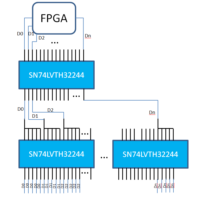
Now the customer has a block diagram to use SN74LVTH32244. Pleas check the attach. 

Is the case correct if the SN74LVTH32244 is used like in the block diagram?

  • Hi Mickey,

    It looks like your customer is using the SN74LVTH32244 for fanout of the D0...Dn signals. This is a fairly common application and should work well. The FPGA should easily be able to drive single inputs on the SN74LVTH32244, and each output of those can drive many inputs on the next stage (typically up to 15).

    The SN74LVTH32244 doesn't directly have a maximum frequency rating, however we can infer from another device that was created on the same technology. The SN74LVTH32374 is a flip-flop built on the same technology (LVT) that does have a maximum frequency rating (fmax(min) = 160 MHz). This means that the SN74LVTH32244 will definitely work up to 160 MHz, however I cannot guarantee operation beyond that.

    Can you tell me more about what they are trying to accomplish? I assume they want to ensure matched timing at the distant end, which is why they have two stages of buffers, but loading will also be a factor in the final signal timing/quality. Are there equal loads on all the D0...Dn outputs?

  • Hi Emrys,

    Thanks for your reply. I will confirm with the customer.