This thread has been locked.

If you have a related question, please click the "Ask a related question" button in the top right corner. The newly created question will be automatically linked to this question.

SN74AHCT1G08: Is there any risk to pull up the output to 12V continuously through a 510 ohm resistor?

Part Number: SN74AHCT1G08

Hi,

In one of My customer's design, the output of 1G08 has to be pulled up to 12V continuously through a resistor. The device is powered from 5V, So the clamp current will be limited to arround 14mA, well below the absolute maximum rating. I wondered is there any risk for this kind of condition? If yes, how about higher resistance value?

Thank you,

John

  • Footnote 2 says:

    The input and output voltage ratings may be exceeded if the input and output current ratings are observed.

    However, any output voltage above VCC is outside the recommended operating conditions, which, in theory, implies that correct operation is not guaranteed.

    In practice, this will not directly affect the AND gate itself, but 14 mA might heat up the ESD protection diode too much over time. Furthermore, if the 5 V supply cannot sink those 14 mA, it might rise to a higher voltage and destroy everything connected to it.

    To go easy on the diode, I would limit the current to something smaller, i.e., 100 µA or so. And to ensure that that current does not affect the 5 V supply, add an appropriate resistor between 5 V and ground.

  • Thank you for reply.
  • Hi,

    A further question. Customer told me, 100uA is impossible. Do you think 10mA (clamp current) is safe or not if the 5V supply is confirmed regulated? Is there any possibility for this clamp current to trig latch-up effect?

    Thank you,
    John
  • Latch-up will not happen inside the absolute maximum ratings.

    I have no information what effect a continuous current of 10 mA has. (And I doubt that this is something TI tests for.)

    I guess the customer doesn't have enough space/money to use a NAND gate and a MOSFET?
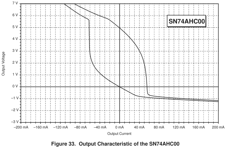
  • The voltage at the output pin will be clamped to ~5.7V (Vcc + clamp diode voltage). From the device's point of view, you are only applying 5.7V with 10mA of current, so you can keep this going indefinitely. The power consumption is ~7mW, so you would expect to see a slight rise in temperature (about 2C), but certainly nothing dangerous to the device.

    Just curious here - but what are they doing that requires the output of an AND gate to be always connected to 12V?
  • The voltage at the output pin will be clamped to ~5.7V (Vcc + clamp diode voltage).

    According to Input and Output Characteristics of Digital Integrated Circuits at 5-V Supply Voltage (SZZA008), the output transistor takes all the current; the clamp diode begin conducting at the voltage that result from about 25 mA:

  • Thank you for confirm.
    It is not due to limitation of space or money. It is due to some wrong insertion of the board in field application. The ckt is on a daughter card of system. It is designed to drive an opto coupller on mother board. There is no problem as long as the card is correctly assembled since the opto-coupller is pulled up to 5V (this is reason why they can not use very high resistance), while there is possibility the card is mistakenly inserted into wrong slot, in this condition the output of 1G08 will be pulled up to 12V. They do not require the device function properly but it cannot be damaged.

    Regards,
    John