This thread has been locked.

If you have a related question, please click the "Ask a related question" button in the top right corner. The newly created question will be automatically linked to this question.

LSF0108: Application for LPC interface

Part Number: LSF0108
Other Parts Discussed in Thread: TXB0108, TXS0108E

Hi,

Customer is using LSF0108 for LPC applicationn from 1.8V (SOC side) to 3.3V (LPC device side.)  LPC is push-pull at SOC side, and open-drain at device side.

The requirement at LPC device side is as below.

  •  VIH =2V Min.
  • VIL =0.8V Max

Now the customer schematics is shown as below.  Do they need to have pull-up resistor at both sides?  Is there any better suggestion regarding how to reach higher level of "output high voltage" and lower level of "output low voltage"?  Besdies, is TXB0108 or any other chip a better option?

Thanks!

Antony

  • The pull-up resistors on the 'SoC side' are likely unnecessary, and they are definitely too small (which is probably why their VOL value is too high) - I would either remove them entirely or replace them with 10kΩ. The 'device side' resistor values can be tweaked to change the VOH a bit -- depending on the speed requirements.  If this is for high speed communication, the 300 Ω resistor might not be low enough, so reducing the value could increase VOH. There's a drawback to this, which is current requirements at the SoC to pull the line low.  The other option for increasing VOH is to reduce line capacitance on the device side as much as possible.

  • Hi Emrys,

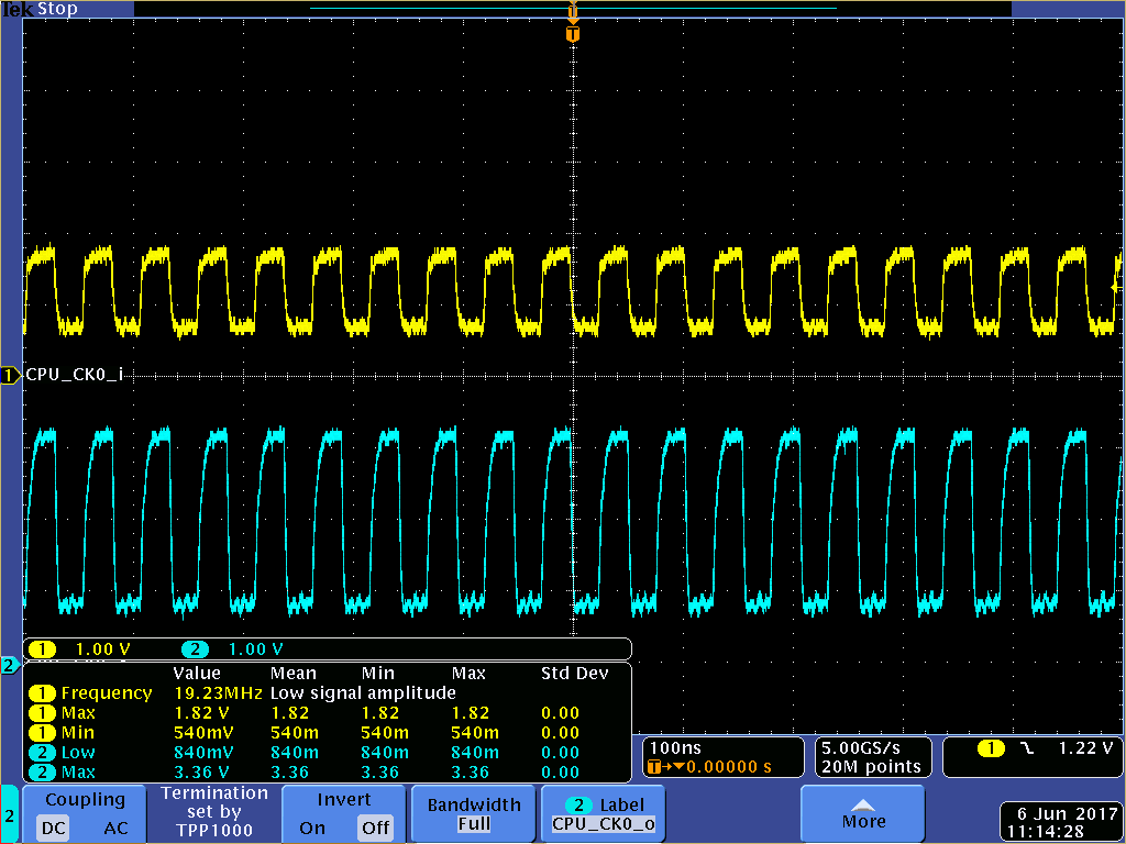
    Please provide your comment for the waveform.

    change B side (3.3V) PU to 1.15K

    Thanks

  • The increased high-side resistance is causing a slower rise time (as expected in this type of translator).

    Additionally, you can see how the reduced current requirement on the SoC has reduce the V_OL significantly.

    These two factors are the balancing act that is required for pull-up resistor selection. As I previously stated, removing the SoC side pull-ups will help significantly by reducing the current requirement at the SoC (as drawn above, it has to sink current from the 150 ohm resistors PLUS the current from the 301 ohm resistors).
  • Hi Emrys,

    If I understood correclty, it's a trade-off between increase VOH and decrease VOL at LPC device side through changing device side pull-up resisotr, right?

    You also mentioned it could be helpful to reduce the line capacitance on their board, but they already try to remove componentes at device side and it's not helpful.  Does it mean this part can't meet their system design requirement?

    If no, if TXB0108 a better fit for customer?  But I see it's not a p2p compatible device.  Please provide all possible ways to improve this at customer side, so that customer can judge what they can do to fix it.

    Thanks!

    Antony

  • Did they already remove the 150 ohm resistors?

    After that, my next step would be to try a 470 ohm pull-up in place of the 301 ohm resistor -- it should maintain similar timing to the 301 ohm resistor and provide improved VOL.

    One additional step that can reduce capacitance is to cutout the ground plane beneath the signal lines - while it's not optimal, it will significantly reduce capacitance and speed up the transitions.

    The TXB device should work fine with this speed and at these voltages, but it is also load sensitive. There is also a TXS0108E that has a very similar pinout and might be drop-in compatible -- we would just have to see their schematic and verify that there aren't any issues.
  • Hi Emrys,

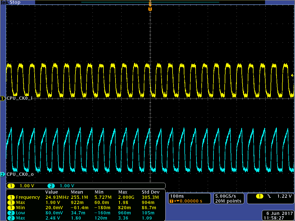
    From the previously attached two waveform plots, the first one is actually captured with SOC side (1.8V) PU removed and device side (3.3V) PU as 150ohm.  Based on your reply, I'll ask them trying to implement 470ohm on device side (3.3V).

    Meanwhile, do you mean TXS0108E would be a better solution than TXB0108 for them?  Both of them are not p2p compatible though.

    Thanks!

    Antony

  • You're right - I saw that the channels and reference voltages align and wondered if we could find a way to make it work, but since the ground pin switches corners it seems that's not possible.

    The TXS device operates very similarly to the LSF, but it contains built-in pull-up resistors and one-shot edge accelerators (to speed up the low->high transition times). i think it would work well for your application.
  • Hi Emrys,

    Please check below for the waveform plot with PU as 470ohm on device side (3.3V), and remove PU at SOC side (1.8V).  It seems not helpful.

    Besides, customers mentioned their LPC function could still be failed when SOC side (1.8V) PU is removed.  The test result is better when SOC side PU is implemented.

    Regarding TXS device you proposed, what would be the external PU you proposed at both sides?

    Antony

  • TXS has internal 10k pull-ups - you should not use external pull-ups.
  • Hi Emrys,

    Thanks!

    May we know what is the major difference between LSF/TXB/TXS family and how should we judge which family we should choose based on custoemr's application?

    Thanks!

    Antony

  • The LSF family of translators are completely passive - they are essentially switches that monitor the input/output voltages and go high impedance when either side has reached the threshold voltage (which is essentially the voltage at VrefA).  The up-translation is completed by the pull-up resistor to the higher voltage.

    The TXS family operates very similarly to the LSF family.  The primary difference is that the device has internal pull-ups and one-shot edge accelerators that improve the up-translation edge rates.

    The TXB family is very different from the other two.  This family has buffers on each channel arranged as shown here:

    The yellow highlighted path shows the normal output of the TXB translators, which can only supply ~20uA, and the red path shows the edge-accelerator that bypasses the 4k resistor for a short time to help improve edge rates.