This thread has been locked.

If you have a related question, please click the "Ask a related question" button in the top right corner. The newly created question will be automatically linked to this question.

Path delay longer than the clock period.

Other Parts Discussed in Thread: SN74LVC1G17, SN74LVC1G14

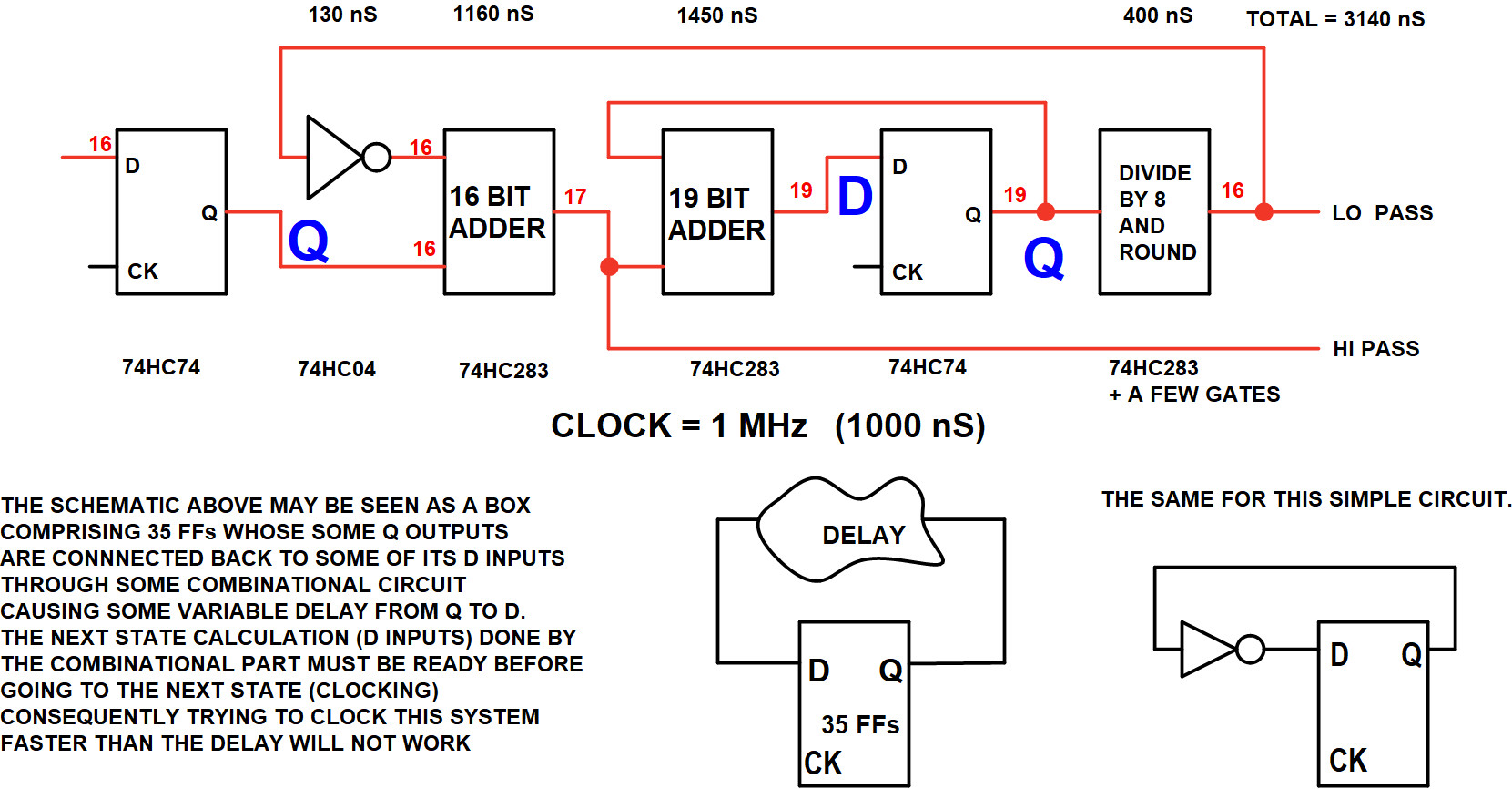
Is it possible that a path delay

(The delay of combinational gates between Q output of Flip Flops (FFs) to the D input of the next stage of Flip Flops)

be longer than the clock period ? 

Can a system works in such a case?  How? 

  • Hello Serge,

    I believe it is possible. If we take the extreme case, then at very very high frequencies the input could be clocked to the output and the next stage could be clocked multiple times before the propagation delay from input to output of the first stage is complete. Although at such high frequencies it is likely that the signal integrity would be very poor, so it may not even work very well at all.

    Is there a particular part with which you are concerned? what are you trying to acheive with the circuit, and what frequency do you intend to operate at?

    Best,
    Michael
  • Hi Serge,
    Can you describe the system in which you have these FFs?

    What type of application are you trying to use them for?

    Do you have a part number?
  • Thanks to Michael J Schultis and Emrys Maier for responding.

    Michael, you are right: it could not work.

    Emrys and Michael, since I cannot attach a file in this forum, I send you a link to a schematic showing the issue.

    www.dropbox.com/.../Filter.jpg

    It is a 16 bit First Order Filter. In this JPEG schematic, lines in red are buses, numbers in red indicate bus width.
    In this simplified schematic, the inverter represents 16 inverters, the 16 bit adder is made from four 4-bit adders, etc.
    Of course, sixteen 74HC74 may be replaced by octal D FFs.

    Delay of each block is written above the block.
    This delay comes from TI's data sheets. (Operating temperature 85 degree, supply voltage 2V, 74HC devices.)

    Components used are named under each block. (Note: The inverter is required to build a substract function from the first adder.)

    The longest path is 3140 nS.
    System clock is 1 MHz, not so high a frequency. (This relatively low frequency is required somewhere else in the system, to process data at higher rates.)

    ---------------------------------

    Is it possible to make this filter work in a 1 MHz system clock environment?

    Your comments and suggestions are welcome.

    Serge Mathieu
  • Hello Serge,

    Are you using a 2V supply? typically these devices are used with a higher supply which would significantly decrease any propagation delay.
    Furthermore you could use devices with much lower propagation delay such as the LVC family of devices, as opposed to the HC family you are using. With some of these functions we even have the AUC family which is optimized for high speed operation and can work well at 2V.

    Best,
    Michael
  • Thanks for your reply.

    Yes I know: But using faster devices would also allow increasing the clock frequency accordingly, and we would have the same question at higher clock frequency: The problem would be the same, with, say, a 10 MHz clock instead of 1 MHz. Let's take for granted that we need down to 2V power supply using the HC family. Is there a way to design a form of pipeline, or some similar trick to make this filter work? (A pipeline would work if there were no feedback.) Some suggestion?

    A demultiplex/multiplex design would also work if there were no feedback. (In an assembly line, a worker takes 1 second to process an item (=propagation delay) . But we need to process 2 items per second. The solution: 2 workers, working either in series, doing each half of the job faster, the first worker transferring his result to the second worker (= pipeline) , or in parallel, each worker accepting the input alternatively, doing both the same job in parallel and giving the output alternatively = what I called DMPX/MPX design) In both cases, there is a on clock delay on the output. I think that both approaches don't work, because of the feedback loop. (Feedback/feddforward loops are often problematic...)

    Any idea to make this filter work? Some trick? Thanks.
  • It seems to me that this circuit is best implemented using an FPGA. Is there some benefit to using a discrete solution that I'm missing here?

    FYI - you (and anyone) can post both images and files on the forum directly. TI employees cannot directly access dropbox due to security precautions on our network, so posting us links to that site really makes it much more difficult for us to help....
  • Emrys, thanks for replying. My initial question remains unanswered: is it possible that a path delay be longer than the clock period. 

    Here is again the  example I used, using 74HC parts. (Delays shown for 85 degree, 2Volts)

    (I hope you can see it. I tried to paste from Word, it does not work: images are not transferred. So I attached a jpeg file.)

    I believe that this 74HC circuit cannot work at 1 MHz. Explanation in the image above. 

    However, in real life, there is no relationship between the system clock of a design and the operating frequency of some part of the same design.

    Even if the system clock has been chosen 1 MHz, (a frequency selected to allow for sampling the fastest signal in the whole application) ,

    various sections of a design could be clocked at, say, 100 kHz, 1 Hertz, or even sporadically on specific, slow events. 

    Let us suppose that the application must clock the filter, only when some condition is detected by a set of combinational gates. Let us name this combinational output "NAME".

    The logic involved to generate NAME (Ex: NAME = A*(B+C+D) + D*(A-NOT+E*F, etc...) is such that it becomes impossible that the frequency of NAME be higher

    than 100 kKz. When NAME comes true, data must be entered into the filter. (Clocking 74HC74 Flip Flops) 

    Unfortunately, NAME is glitched, due to the various gate delays in its logic. 

    My questions are:

    1-How can a 74HC74  be reliably clocked from a glitched signal? 

    The same questions applies not only for the clock input, but also for the reset (set) inputs of a 74HC74:

    2-What to do to reliably reset (set) a 74HC74 from a set of combinational gates, presenting transitory glitches? 

    My objective here is to demonstrate that the actual 74 devices have serious limitations, are difficult to design with.

    However, adding a few new devices to the family, and some simple design rules, will overcome these serious limitations.  

    TI could significantly increase sales of discrete devices. 


  • See my reply to Emrys, thanks,
  • Hello Serge,

    Thank you for your inputs, certainly an interesting topic of discussion.
    If you have specific questions regarding our parts or an application you are working on then feel free to post in a new thread and we would be happy to help!

    Best,
    Michael
  • Michael,

    Thanks for replying.

    Yes, I have questions regarding TI's parts and an application I am working on. But before going further, I would like to get answers for my previous questions. They are:
    1- May the data path to the D input of a 74HC74 be longer than its clock period?
    2- How can a 74HC74 be reliably clocked from a glitched signal?
    3- How can a 74HC74 be reliably reset/set from a glitched signal?

    Our preceding discussions, and the examples I sent, give the whole context of the questions. Let me sum-up the questions 2 and 3 above.

    In almost any digital design, clocking or resetting a FF (Flip Flop) is almost ALWAYS decided by some logic conditions. For example: a counter must be reset when, say, A=47, and B is true and C is false, OR D is less than 100 and .... etc. In any application, the moment to reset a FF is always determined by some combinational conditions decoded by gates.

    BUT: the output of any set of gates decoding some conditions (like the ones above) may be glitched, may have spurious undesired responses, due to gate delays. (Even if all inputs are synchronous: change at the same time.)

    My question is:

    3- How do we reset a 74HC74 Flip Flop (or any equivalent D FF) according to some conditions like the ones stated above, knowing that decoding this condition with gates will generate glitches/spikes (at the output of the decoder) that could (and will) falsely reset the FF.

    2- Similarly, in almost any digital design, clocking a FF (or a whole function like a counter) is determined by some logic conditions decoded by a set of gates. Remembering that decoding with gates could (and will) generate spurious responses and/or glitches, how is it possible to clock a 74HC74 FF from a decoding circuit that could (and will: Murphy's law really works!) be glitched?

    If these two questions are not clear, feel free to ask me for more details.

    As suggested, I also post these two questions in a new thread. I will be back later with the first question .

    Please, tell me the way TI suggests to reset (or clock) a 74HC74 Flip Flop, in the context above .
  • Hello Serge,

    It is possible that the data path can be longer than the clock period, there will just be additional delay in propagation of the signal to wait for the additional period.

    If there is a glitch being generated from the output of a preceding logic device that cannot be removed and may clock the input of a D flip flop, a capacitor could be added at the output of the device to suppress this glitch. Since there will be additional capacitance on the line to suppress such a glitch, it would be recommended to use a schmitt trigger input device to be able to tolerate any slow edges.

    In this way, the glitch is removed into the schmitt trigger buffer, and it generates a clean fast rising edge input into the CLK of the flip flop which should only clock a single time because of this clean edge. A device such as the SN74LVC1G14 or SN74LVC1G17 would work.
    This should help to avoid any issues due to the glitch.

    Hope this helps!
    Best,
    Michael
  • 1- Can a path delay longer than the clock period?

    2- How to control the clocking of a function (a counter for example) using a glitched signal?

    3- How to reliably reset or set a Flip Flop (FF) using a glitched signal?

    4- How a unique signal can at the same time reset some FFs, while clocking others?

    5- How to clock a counter when signal A does a positive transition, or signal B does a negative transition, both A and B are random?

    Suggestion: Texas Instruments should add these devices to her production line. These devices will simplify our lives as designers. 

    www.dropbox.com/.../SyncDesign3.pdf

    www.dropbox.com/.../SyncDesign3.pdf