This thread has been locked.

If you have a related question, please click the "Ask a related question" button in the top right corner. The newly created question will be automatically linked to this question.

SN74LVC2G74: SN74LVC2G74:Q引脚输出问题

Part Number: SN74LVC2G74
Other Parts Discussed in Thread: SN74LVC1G17

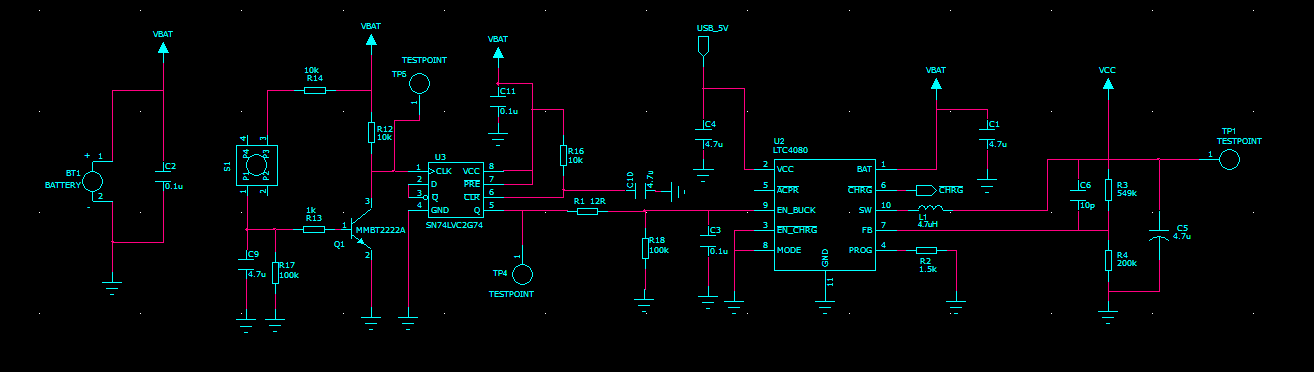
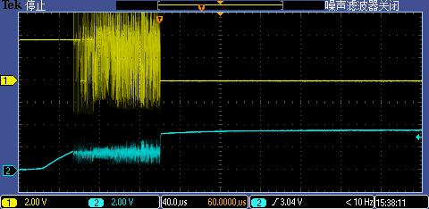
在使用SN74LVC2G74过程中,按键开关能开启电路,即第一次按下去时候Q引脚输出高电平,“Q非”低电平,这是正常的;但是,第二次按按键开关时候,始终无法改变Q引脚的电平(Q引脚一直为高);自己在调试时候发现: 当在“Q非”引脚外接一个负载到地,却又能实现Q引脚电平的正常转换。  查看SN74LVC2G74数据手册,发现我的设计电路与文档中示例并无差异,请问我这问题出在哪里?

  • Hello,

    I translated your question on google to:

    In the use of SN74LVC2G74 process, the key switch can open the circuit, that is, the first time when the Q pin output high, "Q non" low, which is normal;

    However, the second press the button switch, Can not change the Q pin level (Q pin has been high);

    their debugging time found: when the "Q non" pin external load to a ground, but can achieve the normal conversion of the Q pin level

    The Look at the SN74LVC2G74 data sheet and find that my design circuit is not different from the sample in the document.

    What is the problem?

    The indicated part of your circuit should be replaced with a Schmitt-trigger buffer for proper operation.

    The output of the debounce circuit currently has two problems:

    1. Output is a falling edge - clock requires a rising edge. If you prefer to trigger on button release, a Schmitt-trigger inverter should be used.  If you prefer to trigger on button press, a Schmitt-trigger buffer should be used.

    2. Output is too slow for CMOS input. The RC circuit formed with R14 and C9 will produce a slow rising edge into the base of Q1, which will produce a similar curve to the input of CLK.  This slow edge can cause oscillation, excessive current, malfunctions, and damage to the SN74LVC2G74.

    Additionally, it is a good idea to add a Schmitt-trigger to the CLR input for the same reason (R16 and C10 produce a slow edge into a CMOS input).  Our application section does show an RC input there, but this is a mistake and will be remedied in the next datasheet revision. This is not as severe of an issue since it only occurs once when power is applied to the system whereas the button triggers the CLK input multiple times.

    For details on how slow inputs can cause problems, please read: Implications of Slow or Floating CMOS Inputs

  • 您好!

    非常感谢您的回复,您的建议我将在下一个版本方案中应用。

    但是我现在仍然要尝试着调试这块板子,结合您给的启发,首先,我试着将C9和C10这两个电容去掉了,然后用示波器同时检测CLK和Q脚的信号,当按开关时候,发现如图所示波形(上面是CLK信号,下面是Q信号): 从这上面来看,当一个上升沿来到时候,Q脚电平的转变是随机的(有时候能够转变,有时候又不能),这是为何呢?

    第二:如果我CLK引脚不连接示波器,仅仅将示波器连在Q引脚上面,我又发现一个很奇怪的现象:无论怎么按开关,Q脚电平始终为高电平。这让我很难理解?难道连接示波器对我的电路造成了什么影响?

  • Hello,

    I have translated your post to English using a translate tool to:

    Hello!

    Thank you very much for your reply. Your suggestion I will apply in the next version of the program.

    But I still want to try to debug this board, combined with your inspiration, first of all, I tried to C9 and C10 these two capacitors removed, and then use the oscilloscope to detect the CLK and Q feet of the signal, when the switch , Found as shown in the waveform (above the CLK signal, the following is the Q signal): From this point of view, when a rising edge came, the Q pin level change is random (sometimes can change, sometimes And can not), why is this?

    Second: If I CLK pin is not connected to the oscilloscope, just connect the oscilloscope connected to the Q pin above, I found a very strange phenomenon: no matter how the switch, Q pin level is always high. It makes me hard to understand? What is the effect of connecting the oscilloscope to my circuit?

    Hello,

    The problem with removing C9 altogether, is that the switch will not be debounced, and therefore could trigger multiple times very rapidly. You may still need to use the capacitor to debounce the switch, but unfortunately that means you would need to use the schmitt trigger buffer or inverter to overcome this issue as Emrys mentioned in the previous post.

    The effect of connecting the oscilloscope to the circuit is that the cabling and the oscilloscope itself provide capacitance. This capacitance may be enough to have the circuit work under some conditions as you have shown previously, but may not be enough to work always.

    It would be recommended to redesign the circuit, as I am not sure you will be able to have the circuit work using the current setup.

    Best,
    Michael

  • 非常感谢您给的建议。

    我知道这次设计的电路存在一些严重的错误,我也正在制作新的PCB板,采用您的方案,希望下一个版本更好的实现功能。

    但是,俗话说:失败是成功之母!经过这次设计发现的错误,我从中学到了很多知识,所以我这段时间也一直尽最大的努力去尝试着调试,希望改变电阻和电容的阻值,或者外接一些负载,以致于原有的电路能实现期望的功能。

    今天,我做了一个实验:将C9电容阻值改为1uF,一方面能够起消抖作用,另一方面,可以使CLK上升沿更加陡峭。  但是我仍然发现了一个新的问题: 如图所示——(上面一条线是CLK输入的信号,下面一条线是Q输出信号)

    当我按一下轻触开关时候,我发现CLK输入信号下降沿有时候竟然也使Q引脚的电平发生了变化,而一旦我将C9电容再一次拿掉,CLK输入信号下降沿就不再影响Q引脚的输出。 这个问题我想了很久,一直没有找到正确的答案,您能帮我解答一下吗?

  • Hello,

    I have translated your post and posted below including my answer:

    Thank you very much for your advice.

    I know that the design of the circuit there are some serious mistakes, I am also making a new PCB board, using your program, I hope the next version of the better implementation of the function.

    However, the saying goes: failure is the mother of success! After this design found the error, I learned a lot of knowledge, so I have been doing this time the best efforts to try debugging, want to change the resistance and capacitance of the resistance, or external load, so that the original The circuit can achieve the desired function.

    Today, I made an experiment: the C9 capacitor resistance to 1uF, on the one hand to act from the shaking, on the other hand, can make CLK rising edge even more steep. But I still found a new problem: as shown in the figure - (the above line is the CLK input signal, the following line is the Q output signal)

    When I press the touch switch, I found that the falling edge of the CLK input signal sometimes changed the level of the Q pin, and once I removed the C9 capacitor again, the falling edge of the CLK input signal no longer Affect the output of the Q pin. I thought for a long time, did not find the correct answer, you can help me answer it?

    Response:

    The only thing that I can think might be triggering the device on the falling edge is if the falling edge is falling too slowly. If the falling edge falls to slowly then it is possible that the output could see a "false rising edge" due to an oscillation.

    Can you zoom in on the falling edge of the clk pulse? Do you see any oscillations when the falling edge is crossing over?

    The key here is to make sure that the transition time is met during any transition, please see the following specification that I have attached from the datasheet. 

    You should also refer to the following white paper which provides information about potential issues related to slow transition rates:

    http://www.ti.com/lit/wp/slla364a/slla364a.pdf 

    I hope that this information is helpful!

    Best Regards,
    Michael

  • 谢谢你,Michael

    你提供这些对我的帮助很大,让我对这一部分的知识有了更深刻的理解。我认真的学习了你推荐的文档,对我的影响很大!

    今天我又进行了大量的实验,发现了与你说的一样的问题:我的三极管输出的上升沿比较缓慢,在Q脚和CLK引脚用示波器检测到剧烈的振荡。我一直尝试着用电容去抵消这些振荡,但是我发现根本就没办法解决;下面我展示几张示波器截图:(黄色代表Q引脚输出,蓝色代表CLK输入)

    第一张图条件是:C9去掉的时候,CLK上升沿触发时候引脚输出信号的变化;

    第二张图条件是:C9为0.01UF的时候,CLK上升沿触发时候引脚输出信号的变化;

    我始终发现了剧烈的振荡,我原本一直以为这些主要原因是我按开关时候抖动造成的振荡,所以一直尝试着消抖处理,然后到现在还是没有能够成功;

    难道我这一部分电路就没有拯救的余地吗?我感到有点苦恼,虽然我可以重新开始一个新的PCB,但是我仍感到遗憾。

    难道上升沿缓慢造成的振荡的问题必须需要一个触发器来解决吗?有其他解决办法吗?

    最后,再一次感谢您对我耐心的解答,谢谢!

    祝愿身体健康,好运连连!

  • Hello,

    Translation of previous post below:
    Thank you, Michael

    You provide these great help to me, let me have a deeper understanding of this part of the knowledge. I seriously studied your recommended documents, a great impact on me!

    Today I had a lot of experiments and found the same problem as you said: the rising edge of my transistor output is slow, in the Q feet and CLK pin with the oscilloscope to detect a violent oscillation. I have been trying to use the capacitor to offset these oscillations, but I found that there is no way to solve; Here I show a few oscilloscope screenshots: (yellow on behalf of Q pin output, blue on behalf of CLK input)

    The first picture is the condition: C9 removed when the CLK rising edge of the pin when the output signal changes;

    The second picture is: C9 is 0.01UF when the CLK rising edge of the pin when the output signal changes;

    I have always found a violent oscillation, I had always thought that the main reason for this is when I switch the oscillation caused by the oscillation, so I have been trying to deal with shaking, and then still did not succeed;

    Is there no room for me to save this part of the circuit? I feel a bit distressed, although I can start a new PCB, but I still feel sorry.

    Is the rising edge of the slowness of the oscillations caused by the problem that requires a trigger to solve it? Is there any other solution?

    Finally, once again thank you for your patience to answer, thank you!

    Wish good health, good luck again and again!

    Response:

    Yes, any capacitance on the lines connected to the input of the logic device will cause a slow rising edge on the input, and this will cause the oscillation that you are seeing. I don't see any way to salvage the current design without a board change.

    Yes, this slow rising edge is causing these oscillations, and it would be best to fix this with a schmitt trigger input device such as the SN74LVC1G17 : www.ti.com/.../sn74lvc1g17.pdf

    Very happy to help.
    Please let me know if you have additional questions and best of luck with your project.
    Michael