This thread has been locked.

If you have a related question, please click the "Ask a related question" button in the top right corner. The newly created question will be automatically linked to this question.

SN74LVC1G126-Q1: Dual SN74LVC1G126-Q1 Usage

Part Number: SN74LVC1G126-Q1
Other Parts Discussed in Thread: SN74LVC1G125-Q1, SN74LVC1G3157

Dual SN74LVC1G126-Q1 Usage

Hi,

My customer would use two SN74LVC1G126-Q1 as SPDT switch like drawing below.


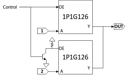
In this circuit, one of the points, we need to take care is the output signal conflict due to delay variation.
It means if we have a device with minimum enable delay (ten) and a device with maximum disable delay (or vice versa), the output signal could be conflicted. Do you think this would be the case?

Other than above mentioned, do you have any other points we should take care?

Thanks,
Ken

  • Hello Ken,

    Yes, as you mentioned, you need to be sure to avoid bus contention between the two devices. In additional to the potential skew between the devices, the top device will likely switch faster than the bottom device due to the delay in the pulldown transistor and pullup structure on the bottom device.
    You could consider using the SN74LVC1G125-q1 since it has an inverted OE. If you tie the different OE signals together then you dont need the additional pulldown, pullup structure, however there still may be skew between the devices.
    Due to this, I would not directly tie the outputs together. I would recommend putting some current limiting resistor between the outputs so that there is not largely excessive current consumption on the output during this short time where there can be bus contention.
    Depending on what you want to limit the peak current to, I would recommend having something like a 500ohm resistor between the two, however, I don't know how important your signal output is and if the 500 ohm would have a significant effect.

    Another device to consider is the SN74LVC1G3157, in which case you don't need to worry about any bus conention at the output since its designed to be an SPDT switch.
    www.ti.com/.../sn74lvc1g3157-q1.pdf

    I hope this helps,
    Best,
    Michael
  • Hello, Michael,

    Thank you so much for your great and prompt reply! It's really helpful for customer (also for me!) to understand what we need to know about this circuit!

    Regards,
    Ken
  • Ken,

    Very happy to help!

    Best,
    Michael