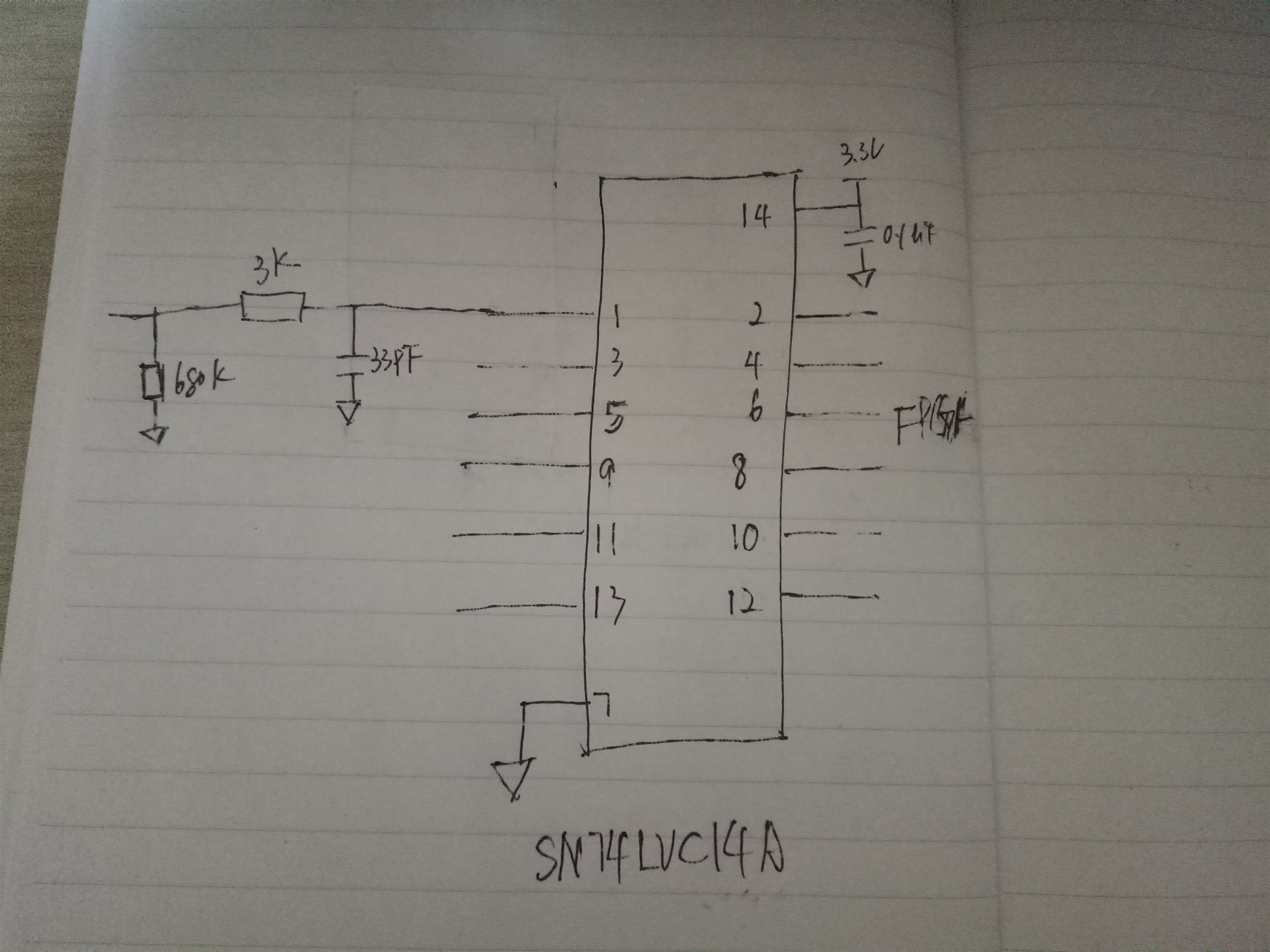
My design is as follows.power supply pin has an 0.1uF bypass capacitor. The 6 channels of the chip are designed the same,Takes channel1 as an example.First pull-down with a resistance which value is 680K, then RC filtering(3K+33pF).All 6 outputs go to FPGA.
Sometimes the output of SN74LVC14A becomes as follow .
I need help.If you can speak Chinese,let me know,thank you .


