A related question is a question created from another question. When the related question is created, it will be automatically linked to the original question.
If you have a related question, please click the "Ask a related question" button in the top right corner. The newly created question will be automatically linked to this question.
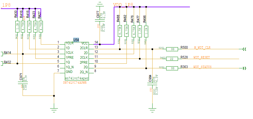
SN74LVC74A: what's minimum time between CLK and /CLR?
The initial state of the flip flop during power up is unknown until a valid input has occurred. In this case , the CLR input is asynchronous to the CLK input , meaning the CLR input overrides the CLK and D input and clears the Q output. however, the default power up state is still unknown.
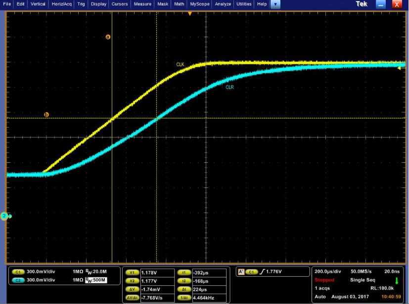
I see that the input clk and clr has very slow rising edge almost 800us for power up which is violating the transition rate requirements. this is because of the 0.1uF cap on the input pins, could you remove it ? Refer to the app note on slow inputs and its effects on outputs. consider using a schmitt trigger to square up the signals. www.ti.com.cn/.../slla364a.pdf
I also notice that the low is not at ground ? am i missing something ?