This thread has been locked.

If you have a related question, please click the "Ask a related question" button in the top right corner. The newly created question will be automatically linked to this question.

SN74LV1T126: Converting a 5 V, 50 MHz clock down to 3.3 V.

Part Number: SN74LV1T126
Other Parts Discussed in Thread: SN74LVC1G17, , SN74LVC2G34

I'm trying to convert a 5 V clock signal running at 50 MHz down to a 3.3 V clock running at the same speed without inverting the clock. I was planning to use a buffer and have it be powered by a 3.3 V source, so when I buffer the 5 V clock, it appears as a 3.3 V clock signal. I started using the SN74LV1T126, and I took the PSPICE model from the product page, imported it into my simulator, LTSPICE, and ran a simulation. Without a load, inputting a 50 MHz clock signal produced a 3.3 V clock at the same frequency at the output. However, when a 50 Ohm load resistor is attached, the output was much smaller, around 1.86 V. I searched around for similar products to the SN74LV1T126, and I found that the SN74LVC1G17 is a similar buffer with a higher current output at 24 mA (at 3.3 V), and its timing characteristics are similar if not better than the SN74LV1T126. Timing is important since the clock signal is fast, so would the SN74LVC1G17 be suitable for my needs compared to the SN74LV1T126? I would have simulated it, but I found that there is no SPICE model for the SN74LVC1G17.

  • Hi Jason,
    Why are you trying to drive a 50 ohm load with a logic buffer? This is rather atypical. Most clock signals drive capacitive (high impedance) loads.

    Can you provide a schematic or explanation of what you are trying to accomplish?
  • Thanks for your reply. I was trying to simulate an SMA port. The resulting 3.3 V clock signal is going to go into an NIM module with SMA connectors, and the connectors have a 50 ohm impedance, so I was trying to simulate it with a 50 ohm load. Here's a link to my schematic thus far:

    drive.google.com/.../view

    In the schematic, you can see the input 5 V clock signal, the output with no load, and the output with a load. I never really designed a circuit like this before, so my plan was to see if a buffer would work like this in ideal conditions, and then I would improve upon the design later on.
  • Logic isn't typically used with 50 ohm transmission lines, but it can be for short distances. You will get a lot of ringing at the distant end due to the impedance mismatch
  • Thank you for your reply. The distance from the source to the load isn't really long, so perhaps this might not be the best model. I'm not entirely sure about the setup, but from what I've been told, the clock will go from the output (when converted to 3.3 V) to the load through an SMA cable at around 3-6 feet. Nevertheless, would the SN74LVC1G17 work for my needs when compared to the SN74LV1T126? Again, I would like to thest the SN74LVC1G17, but I cannot find a SPICE model for it. Based on the datasheet, both buffers seem similar in specifications, but the SN74LVC1G17 has a higher current output (24 mA) compared to the SN74LV1T126 (7 mA). When compared to each other, does the SN74LVC1G17 require any special consideration that the SN74LV1T126  does not?

    EDIT: I went back and reviewed some notes. The distance from the 3.3 V generated clock signal to the input module is around 3-6 feet. Earlier, I said it was 3 meters, but I corrected this measurement after getting more information.

  • In transmission line terms, 'short' would be less than about 10 cm. At 50 MHz and 3 meters, you will see significant transmission line effects. A 50 MHz square wave contains higher frequency components that will have group delay at that range, producing reflections and other issues.  (assuming at the distant end you are connecting straight into a CMOS input (high impedance) )

    [Image deleted, I couldn't get the animation to work on E2E]

    (See animation here: https://en.wikipedia.org/wiki/Square_wave#/media/File:Fourier_series_for_square_wave.gif)

    Here's my recommendation for the best signal quality:

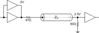
    You can parallel 2 LVC buffers (SN74LVC2G34) and supply them with 5V to produce a fairly low impedance (~5 ohm) output. Adding a series 47 ohm resistor will get close to a 50 ohm source impedance. Then that connects to the transmission line, which is terminated with 50 ohms at the distant end.  This will eliminate the vast majority of reflections and other transmission line issues, but there's one side effect. The final output voltage will be half of the input voltage (2.5V here) (voltage divider between 50 ohm source and 50 ohm load).

  • Thank you for your reply. I sincerely apologize, but I looked some more information about the setup this is intended for. I got the distances wrong. The distance from the 3.3 V generated clock to the input module is 3-6 feet, not 3 meters as I had earlier stated. I'm sorry for the lack of information. Nevertheless, transmission line effects should still hold for this distance, right?
  • Yes, anything beyond about 10cm will start to see significant effects (this is due to the high frequency components of the square waves, usually 300-500 MHz max)
  • Thank you for your reply. Going back to your previous post, I never considered that transmission line effects would occur from a relatively short distance. I will have to speak to my supervisor to learn more about the setup. If there was a way we could reduce the distance from the 3.3 V converted clock to its final input, that would surely reduce the effects onto the clock. Looking at the datasheet, the SN74LVC2G34 that you recommended gives a max output current of 34 mA when VCC is 4.5 V, and to account for any losses through the transmission line, it would have to be powered by 5V. Would it be realistic to use a buffer powered by 3.3 V and have the clock appear at that voltage at the input, or would TL effects reduce the voltage making it worse as the signal moves across the line?

    Also, is there a PSPICE model available for these 2-input buffers? I looked through the catalog, and I found some PSPICE models of 2-input buffers, but they take a max voltage of 2.7 V for VCC, making it impractical for my simulation. I couldn't find one for the SN74LVC2G34.
  • Usually you can get away with connecting a logic gate straight to a transmission line and the ringing at the distant end is considered 'acceptable' - but I have seen many times where it caused problems (multiple triggering, overcurrent, overvoltage, etc).

    You will be paralleling both channels of the LVC2G34 to get ~70mA of maximum (as shown in my drawing). If you power it with 3.3V, then the output will be 3.3V and the output at the 50 ohm termination (after the transmission line) will be 1.65V

    Unfortunately we don't have a spice model for these devices - we are currently working to develop some simple models for people to use, but that's probably a few months away right now. I know there are some models available on the web, but I'm afraid I can't recommend anything outside of TI's website.
  • Again, thanks for your reply. I looked at the LVC2G34 that you recommended and the circuit you posted. That transmission line seems to be the crux of the problem, devices aside. Like you said, the voltage will drop to around half its nominal value, but assuming a TTL voltage logic level input of 3.3 V, perhaps 2.5 V would be within the tolerable range even if it's not exactly ideal. I'll have to test it with a model to be sure.

    Right now, I was focused on a single supply buffer, since I didn't want to deal with two power supplies. However, a thought occurred to me as I was thinking of other solutions. What if instead of single-supply buffer, we used a dual-supply voltage translator with pull up resistors to translate the clock that way, from 5V to 3.3 V? Is there a voltage level translator provided by TI that can support this kind of conversion through the 6 meter transmission line?
  • I'm really sorry for posting so many replies to this issue, but I wanted to let you know about the SN74LVC2G34. I went to the product page to download the HSPICE and IBIS models in an attempt to try and convert them over to PSPICE to use in my simulator, but I couldn't download the IBIS model, and the ZIP folder containing the HSPICE files are encrypted.
  • Again, I apologize, but another concern popped up that I wanted to address here. The initial clock source is 5 V. Assuming that it drops down to 2.5 V due to the transmission line, could you not just simply connect from the original 5V clock to the 3.3 V input? This all has to do with level translation, so knowing the approximate lumped model of the actual transmission line is critical, so if this is the case, there seems to be no need to create a circuit if you know for sure that due to the transmission line, the 5 V 50 Mhz clock will be seen as 2.5 V at the other end.
  • I would think that the 3.3V device at the distant end would recognize a 2.5V output as a logic 'high' - however the exact value there is going to probably be less than 2.5V since the 5V driver most likely will be outputting at less than 5V (due to the high current demand). The datasheet lists a max voltage drop at IOH = 32mA (per channel) of 0.7V (VOH = 3.8V @ 4.5V supply).

    This means that the output of the SN74LVC2G34 could be as low as 4.3V, and the voltage at the distant end (assuming a perfect 50 ohm impedance match all the way down and a lossless cable) will be 2.15V.

    It's probably best to start with a 7V signal if you want to have ~3.3V at the distant end of the cable.

    ***

    You might be interested in this book: www.amazon.com/.../

    It has a great deal of information regarding digital system design from an analog perspective.
  • Thank you for your reply as well as your link to the book. As a beginning engineer with little experience, this book will help in my career. I apologize for bringing it up again, but in regards to your previous schematic with the transmission line, I believe that was when I said that the cable length was 3 meters. I later mentioned that the actual length was at most 6 feet (or 1.83 meters). Now, even though the length is shortened, there will definitely be some transmission line effects, but because the line is shorter, I would imagine that the voltage drop through the line would me much smaller than half (cutting it from 5 down to 2.5 V). Given this new distance, what would you say would be the voltage drop now?
  • The length of the transmission line does not affect the amount of voltage drop - that's kind of the magic of transmission lines. The voltage drop comes from the perfect matching of 50 ohm input to 50 ohm output (essentially a voltage divider).
  • Thank you for your reply. Since this is the case, wouldn't it be better then to power the SN74LVC2G34 with a 6V (or 5.5 V) supply to bring up the output clock voltage where it will be a little higher for acceptable tolerances due to the voltage drop? Also, the input connector at the end is assumed to have a 50 ohm impedance, but since it's part of a larger circuit, wouldn't the expected impedance be smaller? I would assume that it would adjust the input voltage due to slightly mismatched impedances.
  • I can't really explain transmission lines in a post like this - suffice it to say that you should probably google, youtube, or otherwise look into those and try to get a basic understanding.