This thread has been locked.

If you have a related question, please click the "Ask a related question" button in the top right corner. The newly created question will be automatically linked to this question.

SN74AUP1G74: D-FF Does not respond to changes in D-Pin

Part Number: SN74AUP1G74

Hello,

I am using the D-FF with the specified part number in my application.

In order to check if the device is working properly (With lack of EVB) I soldered the device on a PCB I designed and started testing it with an advantest 93K testhead.

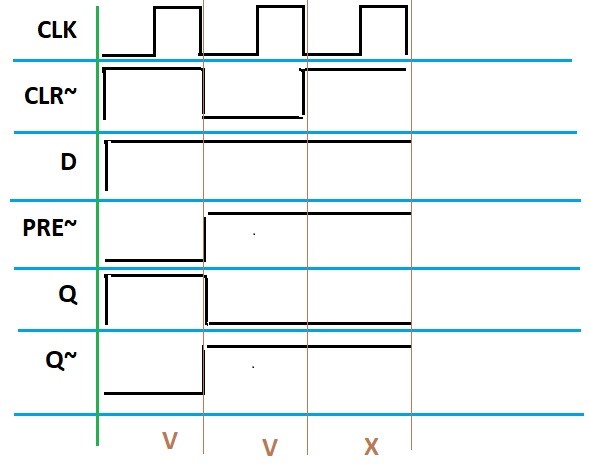
I started by validating Table 1. (Function Table) in the DS (Page 15) row by row and couldn't get it to work.

I started with PRE~ Low and CLR~ High so I got Q=H (As expected)

I then applied PRE~ High-Z and CLR~ Low and got Q=L (As expected).

I then applied PRE~ High, CLR~ High and a 1MHZ 50% D.C. Clock and started changing D (H - L - H - L) - Q isn't changing as expected.

Some devices didn't respond to both D-High and D-Low and some didn't respond to D-Low only.

I would like to know if there is a specific order for changing the D-Pin or if I have to do something in advance.

Thank you.

  • Hi Eli,
    Can you provide a schematic of your test setup and a scope shot of the unexpected behavior?
  • Hello,

    Unfortunately I can't export Photos / Screen shots out of my company.

    During the test the component was soldered to a PCB that gives us access to every pin, The PCB is inserted to a socket that is connected to an Advantest 93K test head.

    I begin with continuity test to make sure that all the pins are properly connected.

    Then the pattern that I run is as described in Table 1. in the DS (Page 15).

    I set the clock to be 1MHz with 50% D.C. with rising edge in the middle (0->1).

    1. I start with Preset (PRE~ = Low, CLR~ = High, CLK = Z, D = Z) - The output Q is High and Q~ is Low as expected. (V)

    2. Then I proceed with Clear (PRE~ = Z, CLR~ = Low, CLK = Z, D = Z) - The output Q is Low and Q~ is High as expected. (V)

    3. Now I want to use D, I apply PRE~ = H, CLR~ = H, CLK = clock, D = H - The output Q remain Low from before and Q~ remain High. (X)

    The problem is that I can't control the device by changing D, the device only change the output using CLR~ and PRE~.

    My question is if there is anything wrong in my flow? Do i have to change something before starting to work with D?

    Thank you.

  • CMOS input pins always must have a valid voltage level; you must not make them High-Z.

    Could you just draw a timing diagram?

  • Hello,

    I added the Timing Diagram picture.

    Thank you.

  • Thanks.

    What are the chracteristics of the input signals? Is ∆t/∆v (section 6.3 of the datasheet) fast enough?

    Some devices didn't respond to both D-High and D-Low and some didn't respond to D-Low only.

    This sounds like a hardware defect.

    It's unlikely but possible that your Hi-Z signals damaged the inputs; but ESD damage is also possible.

  • Hello,
    The timing characteristics is good according to the DS.
    The defects is still appearing in new devices, therefore I dont believe that there is HI-Z / ESD damage.
  • Hi Eli,

    I can tell you that every device that leaves our doors gets tested for functionality, and we have many customers using the SN74AUP1G74 without any problems, so I doubt the problem is with the design of the parts.  I'm not saying it's impossible, but it's very unlikely that the issue is with the IC.

    It sounds to me like you might have excessive capacitance in your test setup that is causing the inputs to be slower than you would expect - at 1 MHz even a few pF can cause big problems.

    Can you provide scope shots of the waveforms at the inputs and outputs of the SN74AUP1G74? We need to know exactly what is happening at the pins to determine what the problem is.