


My customer is powering up the SN74HC259N and there is a “glitch” in the power up ramp. This can be seen below:
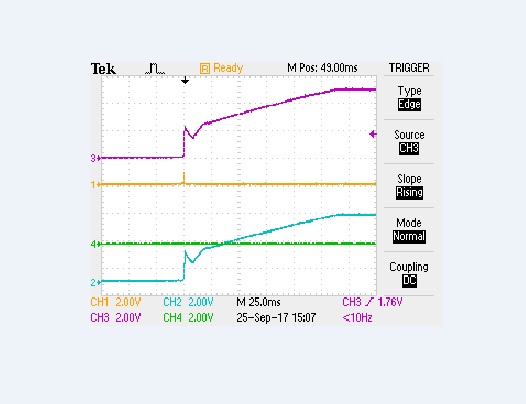
Red +5 Volt
Yellow \CLR
Green Q0
Blue \E
You can see from the pictures that the \CLR signal (pin 15) is held low starting from about the time the power reached 1 Volt, until the processor started running. The Output pin chosen for the pictures was Q0, which is the same as all eight outputs during startup.
Would this cause an issue with the chip? I have seen other chip sin the past where a glitch like this can cause issues with the IC. The customer does not see failures all of the time.
I have attached the schematic below (page 2):
SN74HC259N Vcc Ramp Glitch_10373F2.pdf
I will give some more background on this issue:
The BIU testing process only involves applying power to the product while it is at room temperature. At power up, the \RESET or \CLR inputs are at an active low state. Shortly thereafter, \CLR goes inactive, and the Address, Data, and the \Enable inputs are exercised and the outputs are tested for the proper indication by switching the 24 Volt outputs from the ULN2803s back to the 24 Volt input circuits consisting of the resistor dividers and 74HCT251 Input Multiplexers. Many combinations of binary values are checked during multiple load and latch operations.
Also, we have run an additional test on product that passed previous room temperature testing. The group of 80 units with no power applied was placed in a temperature chamber set to 70 ° C and left overnight. Over 10% of the units failed the same room temperature test the next day. The observed fault was a failure of one or more of the HC259 output pins.
You are correct that the only connection to the HC259 output pins are ULN2803 input pins.
The SN74HC259N ICs are soldered onto the 10373 board.
All of the SN74HC259N output pins connect to ULN2803 Darlington Transistor driver ICs. The failure that we are seeing is that we find some number of the SN74HC259N parts have a non-functioning output pin (or pins) upon the initial test of the board. The boards are placed in an oven and heated to 65 C for three hours and retested after cooling down. We typically find additional SN74HC259N failures during this second test. I have also noted that one of the SN74HC259N parts on a unit that I was examining had a failed output pin, and after additional checking with a scope probe and after a couple of power up – down cycles, the same IC now had an additional failed output pin.
We have another product that uses the same combination of 74HC259 latches connected to ULN2803 drivers. This product has the SN74HC259N ICs installed in sockets, so the parts do not experience the thermal stress of the soldering process. It is very rare for one of the 74HC259s to fail in this other product (typically less than one per thousand). We use many thousands of the parts each year in this product. Also, this product has its final test while it is operating overnight at 65 ° C in a temperature test chamber.
This is why I have concerns about the parts that have been machine soldered.
FYI: I have not seen an instance of the voltage on an HC259 output pin exceeding the +5 Volt power on Pin 16. As the ULN2803 data sheet indicates an equivalent circuit impedance of about 2700 Ohms from the input pin to common, I don’t see how the approximately 2 mAmp load (or even 16 mAmp with all outputs high) would damage the HC259.
The \CLR input is connected to the output of a microprocessor/ watchdog timer control IC and has a pull up resistor to +5 Volt . The part starts to operate once the +5 Volt bus reaches about one volt, and at this time the control IC activates its output. Keeping the HC259 outputs low during startup is a requirement of our application.
Our product operates from +24 VDC, and the ‘glitch’ in the power up sequence occurs because the electronic circuitry does not represent a uniform resistive load. The +5 Volt power is generated by a LM2595T-5 switching regulator IC.
The \E signal to the HC259 comes from an output pin of a 16V8 PLD. The \E signal cannot get to +5 Volts faster than the +5V bus!
All eight of the Qn output pins are held low during startup because the \CLR input is active. The ULN2803 Darlington buffers connected to the HC259 outputs have a typical input leakage current of 65 uAmp. when in the low state. I have not measured the leakage current.
The specified operating voltage range of the HC259 is 2 through 6 Volts. During the power up ‘glitch’, the voltage passes 2 Volts and falls to a value slightly above 2 Volts, before continuing upward to 5 Volts. Since the Vcc voltage remains within the operating voltage range after passing 2 Volts, I don’t see how this could be a problem. You mentioned that the Vcc voltage “does not ramp up properly”. Do you have a document that specifies this?
The customer feels that this is a soldering issue, but I have my doubts. Can the “glitch” cause issues with this chip?
Thanks for your help with this!
Richard Elmquist

