This thread has been locked.

If you have a related question, please click the "Ask a related question" button in the top right corner. The newly created question will be automatically linked to this question.

SN74LV1T125: MOS implementation of SN74LV1T125

Part Number: SN74LV1T125
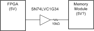
Other Parts Discussed in Thread: SN74LVC1G34, SN74LVC1G07

Plan to use SN74LV1T125 in new programs and as part of that i am looking MOS implementation of this part inorder to interface external logic

  • Hi Raveendra,
    Welcome to the E2E forums!

    I don't completely understand your request.

    What are you trying to interface this part with?

    A schematic of your desired circuit is the best way to describe this, preferably including all supply voltages and part numbers for devices connected directly to the device. The "Insert Code, Attach Files and more..." button at the bottom right of the response box allows for adding images and other files to your post.
  • using FPGA and Memory in some of the designs in where FPGA is driving a signal (configured as Output) and connected this signal to Memory device having signal type of Bidirectional (IO) . I want the signal flow from FPGA to Memory only but NOT from Memory to FPGA. To avoid the signal flow from Memory to FPGA am looking for an external component which can block. Will the SN74LV1T125 works? If I use SN74LV1T125 then when the Memory is driving a signal how is the behavior of SN74LV1T125? To analyze this function asking CMOS implementation of SN74LV1T125. Hope its clear now
  • Thanks, I think I understand now.

    The SN74LV1T125 has a push-pull output implementation, which means it will essentially connect the output directly to Vcc or to Gnd, and if the memory module attempts to drive the line, there will be bus contention. Bus contention will cause excessive current in both devices, and could cause damage.

    Do you not have control over the memory module? I mean, does it just randomly try to output data to a port where you are only trying to input data? That sounds very odd to me.

    If you know when the port is going to switch (ie if the system has an indicator signal for the memory direction) then you can put the SN74LV1T125 into a high-impedance mode, and then there won't be any problem.
  • Thanks for the quick response.
    The FPGA driving the signal randomly to Memory device depends on certain SW conditions.
    when the Memory device receives as input signal from FPGA then memory device will be busy for certain operation and during this time it outputs same signal (Since bidirectional signal to Memory) as a busy condition. I don't want the output signal flow from Memory device to FPGA. Can I achieve this function using SN74LV1T125 by shorting pin No1 (OE\) and pin No 2 (A) and connect to FPGA output signal and Pin No 4 (Y) connect to Memory device Bidirectional input signal?
    With the above mentioned connections, whenever the memory device output the signal is there any signal contention and draw more current from VCC to GND?
  • The way you've described the connections, the SN74LV1T125 won't be able to drive the line HIGH - ever. When the input (A and OE\) goes HIGH, the output will go into high-impedance mode, essentially disconnecting the device.

    I would recommend just adding a resistor in series (1k to 10k) with the output to protect it. When the memory module tries to drive the line to a different level than the SN74LV1T125, the resistor will limit the current and prevent damage to either device (as long as the resistor is large enough to limit the current to the drivers' maximum current values). When the memory is in the 'receiver' mode, the resistor shouldn't cause any problems since the input is high impedance.
  • The signal which FPGA driving is ACTIVE LOW signal and not worried when driving it as HIGH.
    Main worry is whenever Memory device driving (ACTIVE LOW) as soon as it receives input from FPGA then there is signal contention and is there anyway to arrest at this scenario?
  • Are you trying to say that the line will never drive high? That would be a very odd logic system. That's not what 'active low' means. Maybe I'm misunderstanding?
  • FPGA driving the signal (Output only) and has two states logic 0 (0V) and Logic 1 (5V) and connected to Memory Signal (IO). The memory does some operation whenever receives as Logic 0 signal from FPGA and it does not do any operations when it received as Logic 1 signal. The moment when Memory receives the signal as Logic 0 and it starts doing some operations during this time it wants to send same signal as output which I don't want and would like to arrest this signal as output from Memory to FPGA. Is there anyway to block this using any discrete circuit from TI?

  • Hi Raveendra,

    The below circuit will prevent damage to the FPGA and the Memory device. If you need voltage translation, the supply of the SN74LVC1G34 can be selected to match the memory module and it will down-translate the signal.

    The 10kohm series resistor is used to prevent excess current when the memory module is attempting to drive the same line as the SN74LVC1G34.

  • Memory module also a 5V device. adding current limiting 10K resistor in series during signal contention is advisable for Aero applications? Or do you suggest some other glue logic device from TI?
  • There is no device that is designed to protect a push-pull output from bus-contention.

    It is up to the system designer to avoid this situation, or to develop a work-around (which is what I have provided above).
  • have gone thru SN74LVC1G07 and looks this part is best choice to interface between FPGA and Memory device since I am interested Active low input to Memory only. And this device blocks when Memory sending as an output since it supports open collector.  Any comments?

  • The SN74LVC1G07 has an open-drain output, which means that it will force the line LOW at the memory device. If the memory device attempts to drive the line HIGH, then both devices will suffer damage.

    I have already provided the correct solution.
  • Memory never drive High during the period FPGA driving low signal. 

    Memory device has weak internal pullup of 100k, so few 50 Microamps current flows from 5V (of Memory) to GND (when both FPGA and Memory are driving LOW signal at a time) for a short duration of say below 5ms (application requirement) worst case. Is this fine right?

  • Yes, that will be fine.
  • thank you for your support