This thread has been locked.

If you have a related question, please click the "Ask a related question" button in the top right corner. The newly created question will be automatically linked to this question.

SN74AVC4T774: B2 shorted to GND

Part Number: SN74AVC4T774

Hi Team,

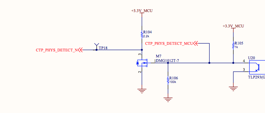
My customer is using the SN74AVC4T774 and are observing that one of the signal inputs on the B side (B2, pin 13) becomes shorted to GND internally in the IC. The B side is 3.3V side, and the A side is 1.8V. The 3.3V side is coming from a separate board (short cabled interface). GND is also passed over the cable. The signal is being pulled up to a different 3.3V power rail than the IC is on. Please see the attached schematic below for reference.

What might we be doing that could cause the chip to develop an internal short to GND? I am wondering if perhaps we are diode conducting on that pin, or if maybe the power sequence is wrong? 

One thing to note is that the /OE pin is directly connected to the SoC (i.e. there is no pullup resistor), but we believe this probably doesn't justify the issue.

Any help or suggestions you can provide is greatly appreciated.

Thanks,
Mitchell

  • Mitchell,

    I see that the DIR1 and DIR 2 are connected to GPIO. What is the status of it? The DIR3 &4 is directly connected to 1.8V which enables A to B signal transmission.
    I do not see the pull-up on the B lines as you have mentioned , are there pull-up resistors on B2 line which is always at 3.3V from a different rail?The Input lines are overvoltage tolerant, however the output lines wont be. If B is setup as output, there could be differences between Vccb and external 3.3V rail which can turn on the internal clamp diode, however, minor voltage differences would not cause it to short to gnd.
    if you can send a scope shot of the input /output signals, will be helpful as well.
    I would not think any power sequencing nor OE pin is causing this to short to gnd. Is this happening as soon as device is put into the board or after sometime ? did the customer try multiple devices too while maintaining proper ESD procedures?most likely could be caused by ESD mishandling.
  • Hello Shreyas,

    Thanks for you help. I will check and see the status of the DIR pins as well as some scope captures.

    I've attached another schematic shot that shows the pullup on B2 (AC_GPIO_2_3V3 is connected to CTP_PHYS_DETECT_N). It is connected to a different 3.3V source, but I think that should be acceptable.

    Thanks,

    Mitchell

  • Mitchell,

    correct me if I'm wrong, but isn't the Nchannel turned on with the gate high through the 3.3_MCU supply? with this, the line is shorted to gnd with 2.2K resistor limiting the current.