This thread has been locked.

If you have a related question, please click the "Ask a related question" button in the top right corner. The newly created question will be automatically linked to this question.

SN74AUP1G17: Frequency Limitations

Part Number: SN74AUP1G17
Other Parts Discussed in Thread: SN74AUP1G74, TINA-TI, SN74LVC1G17, SN74LVC1G14, SN74AUC1G17

Hi Team,

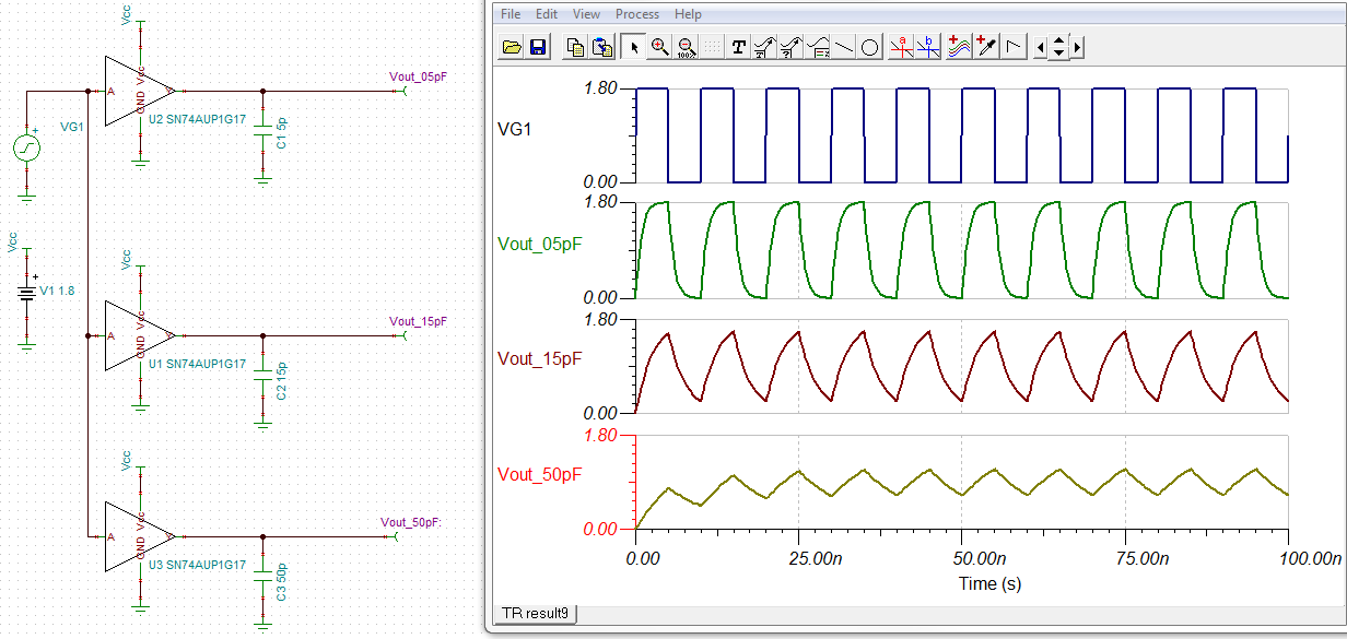
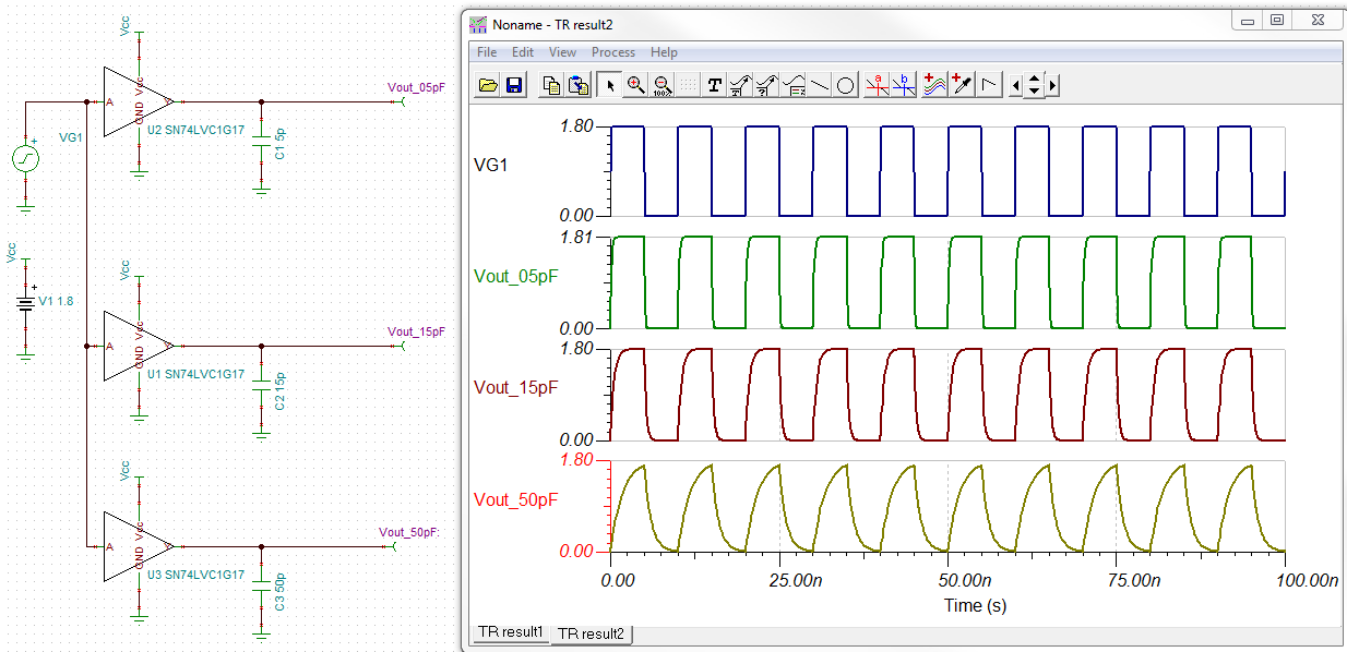
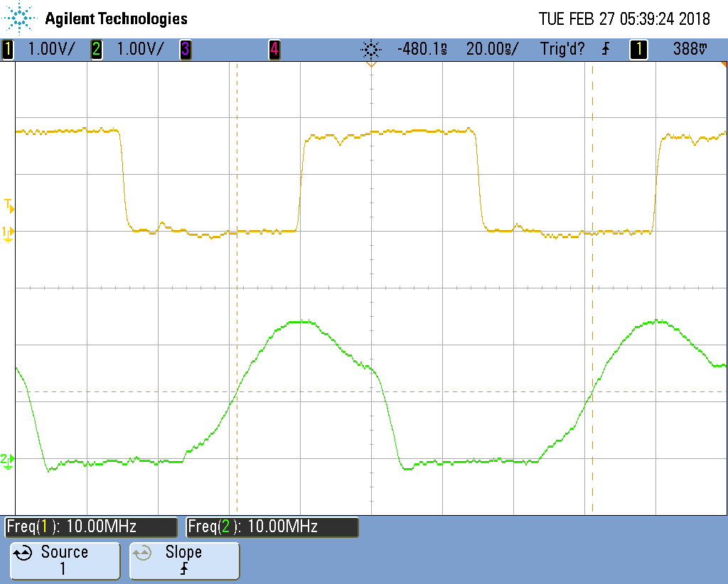
Is the SN74AUP1G17 capable of a 100MHz clock driven through it? What information in the datasheet can be used to determine frequency limitations if any? My customer is expecting to see a square waveform but instead it sounds like they are seeing a non-square waveform with dc offset attached to it. The device is operating at 1.8V. I have asked for a screenshot of the waveform, but wanted to get this question posted in the meantime.

If the SN74AUP1G17 is not capable of 100MHz, can you suggest a P2P device that is? The package is SC70.

Thanks,

Joe Stephan - FAE

  • Hi Joe,

    I hope things are going well for you.

    The question of maximum speed for buffers is so common that we added a Frequently Asked Question for it, located here:

    For this device, I would refer to the SN74AUP1G74 - a clocked device in the same family.  The maximum frequency capability will depend heavily on the capacitive loading on the output.  Since this device has a relatively high output impedance, the output capacitance would have to be very low to reach 100 MHz, ie <= 5pF.

    I made a quick simulation to show the difference loading has on the output:

    And here's a copy of the Tina-TI file if you want to play with the simulation yourself:

    SN74AUP1G17_behavioral_model.TSC

    If you want a part that can just drop in replace and run faster, try the SN74LVC1G17. It has lower output impedance, so runs faster at the same loading.

  • Hi Emrys,

    Thank you for the quick response on this! I hope all is going well for you too.

    Feedback from the customer is that their waveform is looking more like the 50pF sim you provided. Do you have a TINA model for SN74LVC1G17 as well? I wasn't able to find one. I'd like to run sims with LVC version to show the customer.

    Thanks!

    Regards,

    Joe
  • Hey Joe,

    It should be noted that the above model is based on the datasheet specs -- ie the output impedance is the absolute worst case.  It's likely that their load is heavier than 50pF since real devices typically have lower actual impedance.

    I can throw together a similar simulation for the LVC tomorrow when I get into the office. These models are really just behavioral spice models -- if you take a look inside of them, you can see how they are built (basically I just plug in appropriate input thresholds and output impedances). I'm just trying to say that the results are good for a proof of concept, but they definitely aren't perfect representations of our parts. 

  • Hey Joe,

    I put together a model for the SN74LVC1G17 using bench measured values (ie typical values).  Here's a screenshot:

    And the Tina-TI file I used:

    SN74LVC1G17_behavioral_model-typical.TSC

  • Understood. Thank you for your help!

    -Joe
  • Hi Emrys,

    Looks like the SN74LVC1G17 still isn't going to be fast enough. Below shows the output waveforms of the AUP and LVC devices. Do you have any part suggestions that will run faster? Don't worry about it being P2P this time.

    AUP1G17

    LVC1G17

    Thanks,

    Joe Stephan

  • Are you able to tell me more about the application? What are they driving?

    My immediate thought is to parallel two LVC drivers (only parallel channels inside the same chip), since those are the strongest we offer.
  • Emrys,

    The signal is a clock signal that feeds into a FPGA. About 3 inches of trace. The calculated effective load capacitance is <20pF.

    Voltage -1.8V
    Frequency - 100MHz

    Thanks,

    Joe
  • Based on what you're saying, we should be seeing a pretty clean signal, but with some overshoot because the driver is too strong.That doesn't add up with what we're seeing on the scope shots. Is there any chance there's something else loading the line down? Or perhaps a trace is cracked or a solder joint is cold/fractured?

    These device typically have no problem with light loads at 100 MHz. I did see recent case where an ESD protection device was loading the circuit very heavily and distorted the waveforms. Is there anything else on the line? There's got to be some factor we aren't seeing.
  • Emrys,

    Feedback I have recieved is that their is a 25k pull-up internal to the FPGA on the line. That is the only other loading of the line. They are investigating using two in parallel. Do you have any feedback/suggestions?

    Thanks!

    Regards,

    Joe Stephan

  • I should still have some samples sitting around for the LVC1G17 -- I can run 100 MHz through it on a 50pF load in the lab and show how it's supposed to look on Monday.
  • Hey Joe,

    First off - I was wrong.  Sorry for that.  This device won't be able to drive 100 MHz at 1.8V.  I was so focused on what I thought was a heavy output load, I didn't see the incredibly obvious answer that the supply voltage is just too low to support that speed (for LVC or AUP).

    **Update - I forgot to mention that I tested an SN74LVC1G14 - which is the inverting ST buffer.  It has extremely similar behavior to the SN74LVC1G17 **

    After testing in the lab at 55pF (I got as close to 50pF load as I could) I found that there was an important factor I was ignoring at 1.8V operation -- the internal delays. I don't think this device will be able to drive 100MHz even with multiple drivers in parallel. Sorry for leading you down the wrong path.

    The LVC devices work great up in the 3.3V and 5V range, but down at 1.8V, the FET delays start to diverge and the resistances increase.  My behavioral PSpice model doesn't show this behavior, so the simulation results above are not valid.  Here's a scope shot at 2.5 MHz to show the propagation delay:

    Note that the delay shown is ~35ns, which is longer than the whole period of the 100 MHz signal (10ns).  While propagation delay and max frequency are not 100% linked, it's probably a bad idea to try to drive a signal 3x faster than the device's internal delay.

    And here's another scope shot at 10 MHz -- I probably wouldn't try to go faster with ~50pF load:

    I would recommend trying the SN74AUC1G17.  This device is optimized for 1.8V operation and has delay in the ~1ns range.  With a light load (~20pF) you should see delays in the 1 to 2ns range.  It should be a pin-to-pin replacement for the existing solution.