This thread has been locked.

If you have a related question, please click the "Ask a related question" button in the top right corner. The newly created question will be automatically linked to this question.

LSF0108: Rise time is too slow?

Part Number: LSF0108
Other Parts Discussed in Thread: SN74AVC4T774, LSF0102, TXB0108

Hi,

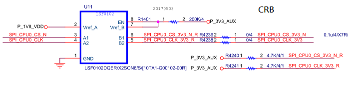
Customer is using LSF0108 for 8MHz SPI application from 1.8V to 3.3V with schematics below.

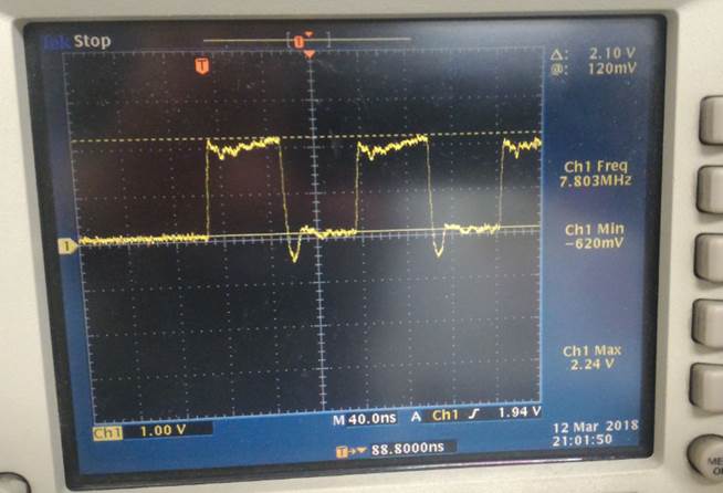
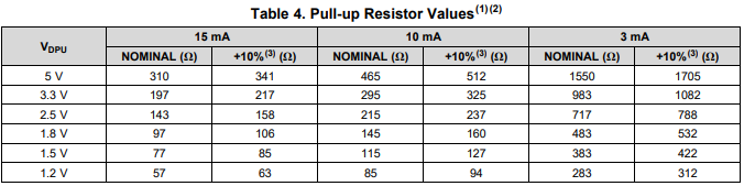
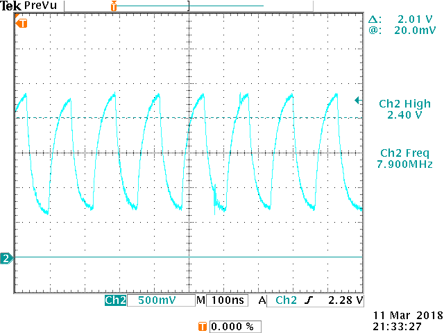
But, they found the output signal can't reach 3.3V and it seems to be a too slow rise time.  The waveform as below is at output side (SPI clock) after they change output side pull-up resistor from 1Kohm to 200ohm.  (With original 1kohm, the rise time is slower.)  I think LSF0108 should be able to cover 8MHz of speed.  What should they do to oversomce this issue?

Thanks!

Antony

  • Hi Antony,

    The LSF devices are passive so they don't provide any drive strength. This leads to issues such as this when the RC delay is too high for the data rate. 

    This link will take you to one of our great training videos over the LSF device which focuses on this issue in particular.

  • Hi,

    Do you mean the customer issue is because the B-side RC is too big?   What is the minimum R can be used here?  The previous waveform is based on pull-up resistor @ 200ohm.  Can it be further lower?  Regarding the C (parasitic capacitance), is there any way that customer can judge how big it is?  If the rise time is still too long based on the minimum R value customer can use, should we suggest other TI component with driving capability?  Which one will you suggest?

    THanks!

    Antony

  • Antony,

    Do you mean the customer issue is because the B-side RC is too big? Yes since the output is controlled by the passive components on the line.  

    What is the minimum R can be used here?  The previous waveform is based on pull-up resistor @ 200ohm.  Can it be further lower? Table 4 in section 9.2.1.2.2 of the datasheet gives recommended resistor values to use. The section itself covers design considerations when choosing the resistor.

    Regarding the C (parasitic capacitance), is there any way that customer can judge how big it is?  Depending on their set-up and equipment it could be measured. Their layout could be a huge factor in this problem for example if they are running long traces that increases parasitic capacitance and resistance. There are tools for calculating parasitics of traces. 

    If the rise time is still too long based on the minimum R value customer can use, should we suggest other TI component with driving capability?  Which one will you suggest? The LSF0108 is a good for bidirectional translation. For SPI applications (knowing the direction of the signal), the SN74AVC4T774 could be a better fit.

  • Hi Dylan,

    Thanks for your reply.  In parallel, the same customer has another board using LSF0102 with schematics and B-side signal waveform as below.  They can't reach 3.3V at B-side as well.  From the waveform, it seems a different issue from above case??  What is the issue for this case?

    Thanks!

    Antony

    Antony

  • Hi Antony,

    This could be due to a weak pull-up. If i'm not mistaken they are using 4.7k resistors which is bigger than recommended. Tell them to try a resistor from the table below (3.3 V row & +10% columns) and see if that helps any. If it doesn't come back to me and I'll continue to try and debug their problem, thanks.

  • Hi Dylan,

    Thanks,.  I'll ask them to try this and let you know the result.

    In parallel, they have one related question of using LSFxx for their uni-direction SPI application.  The question is, at either A-side or B-side, is it necessary to implement external PU resistor on these SPI signal?  Is there a possibility to remove the external PU resistors?

    Thanks!

    Antony

  • Hi Dylan,

    After cross checking with the customer, let's skip the discussion about the case for LSF0102 since it's on CPU ref design board instead of customer's board.  So, let's just focus on the LSF0108 case that is mentioned in the beginning.

    One first question is, do you see any concern that they didn't connect EN pin to Vref-B as mentioned in the datasheet?

    Today we receive some more waveform as below when pullup resistor is 200ohm at B-side.

    • The first waveform is captured before they power up their system, and you can see 3.3V at these signals.
    • The 2nd waveform is captured after system power up when there's a SPI access.  You can see the high level is only around 2.4V and low level is around 720mV.
    • Meanwhile, when they tried 100ohm pullup resistor, high level voltage is around 2.8V.
    • When they tried kohm pullup resistor, high level voltage is around 2.1V
    • The 3.3V SPI signal is connected to an SPI flash with VIH@2.31V and VIL@0.8V.

    Do you see any possibility to improve this using the board design they have now?  The project is closed to the final stage and they may not be able to change layout design.  I tried to check TXS0108 and TXB0108, but found the it's not drop-in replacement (TSSOP package.)  Please share your inputs how we can solve this.  THanks a lot!

    SPI_FLASH_CLK:

    High level: 2.41V

    Low level: 720mV


    SPI_FLASH_MOSI:

    High level: 2.43V

    Low level: 720mV

    Antony

  • Hi Antony,

    Not connecting the EN and Vrefb through the 200kohm is definitely a problem which needs to be fixed.
    The bias point is not fixed when you have 200k on Vrefb but not on En.
    The transistors are biased at 3.3 when En is directly connected instead of ~2.4V when properly connected. The threshold change will affect the switching especially at higher freq.
    I highly encourage watching the LSF videos about up/down translation and biasing.

    Having lowered pullup resistor affects the Vol at the output since there is additional current generated which needs to sink into the host; hence the vol is ~750mV.

    For push pull signals, there is no need for pullup resistor on the host side.

    Would you /customer consider using a SN74AVC4T774 device specifically made for SPI communication with DIR pin for each io pin.