This thread has been locked.

If you have a related question, please click the "Ask a related question" button in the top right corner. The newly created question will be automatically linked to this question.

SN74AVC4T774: Current Consumption Too High

Part Number: SN74AVC4T774
Other Parts Discussed in Thread: CC2564MODA, BOOST-CC2564MODA

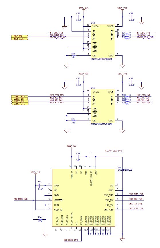
I'm using the CC2564MODA DUAL Mode Bluetooth Module in a new design and am finding that the power consumption when the bluetooth module is in Shutdown mode is higher than excpected, about 3mA all together. I believe that the source of the higher current consumption is the level shifters I'm using, the SN74AVC4T774RSVR. I know that the Bluetooth is in shutdown mode because the Shutdown enable line is driven to ground. I have been comparing the module I'm developing with and without the Bluetooth hardware and the module without Bluetooth hardware installed doesn't draw this extra current. When I tried disabling the outputs on the level shifters using their output enable pins the current draw only increases. I have also been comparing my modules current consumption to that of a development board I purchased from TI, the BOOST-CC2564MODA, I removed the level shifters from that dev. board for comparison and didn't see a difference in the current draw, so perhaps the Bluetooth module is drawing the extra current after all. Is there a schematic available for this dev. board? I haven't been able to find one as yet. Below if have attached the Bluetooth Portion from the schematic for my design. I also used documentation from the TI wiki site as a reference regarding the Bluetooth modules integration with these level shifters.

  • Hi Michael,

    Welcome to e2e!
    Thanks for the detailed explanation and schematic provided.
    I see that the DIR1 is tied to Vcca such that signal flow is A to B. When the level shifter is disabled, the input circuitry is still active and hence I will suggest having the B port tied to ground as well.
    It is true for all the other IO ports as well. When Hi-Z, the IO ports will have its input circuitry active. you can try having the IO ports with weak pull-down resistors to see if the Icc current goes down.
  • Given this new information and per my schematic. For the signal channels that have DIRn pulled to GND such that the signal flow is Bn->An I should connect a weak pull down resistor(~100kΩ) between Bn and Ground to force the Input circuitry into a low power state. If this seems right to you I will try it out on the bench an report back with my findings. The CC2564MODA Bluetooth module enables it's own pull-ups on the UART and Debug pins when in shutdown, assuming 1MΩ for those pull-ups I believe 100kΩ pull-downs should be sufficiently weak while holding the input signals within the level shifters' VIL threshold.