


Other Parts Discussed in Thread: SN74AUC1G17
Hello,
I'm using this part to receive a trigger that could have a slow rise time. The intention is to use this part to provide clean rising and falling edges to the next IC in line. I have a few questions though.
ch1. is the input
ch2. is the output
1. Where do you find the rise/fall times (slew rate?) in this data sheet? It doesn't seem to be listed.
2. I'm testing with this part now and the below screenshots of operation with a 1Mhz square wave input (3.3Vpp with Vcc = 3.3V) from a TEK sig gen raise some questions.
a. Why is the output so noisy?
b. The rise time seems to be ~10nS. Does this make sense? I'm trying to reconcile this with the data sheet.
3. Why does section 10.2 reference a (delta t)/(delta V)? I cannot find this in the datasheet.
Note about schematics: The part is implemented on a PCB with NO decoupling cap (this could be contributing to the noise seen in Ch2 (red)??). There is no output cap and no input cap on the input/output pins. This part is driving a clock input of another IC that does not list a spec for this pin's input capacitance.
fig1
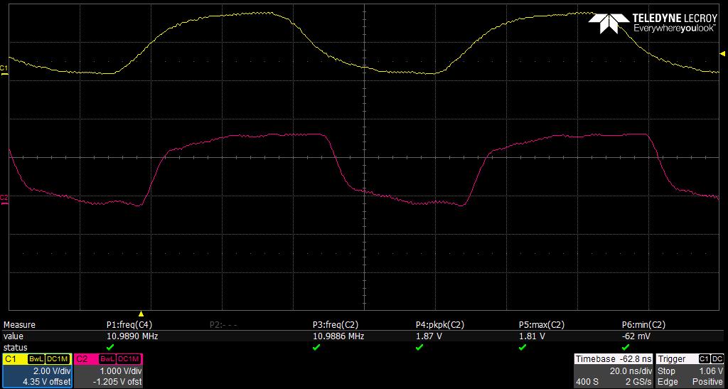
fig2


