This thread has been locked.

If you have a related question, please click the "Ask a related question" button in the top right corner. The newly created question will be automatically linked to this question.

TXS0108E: OE and glitch

Part Number: TXS0108E

Hi TI support,

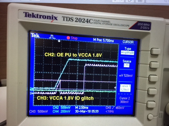
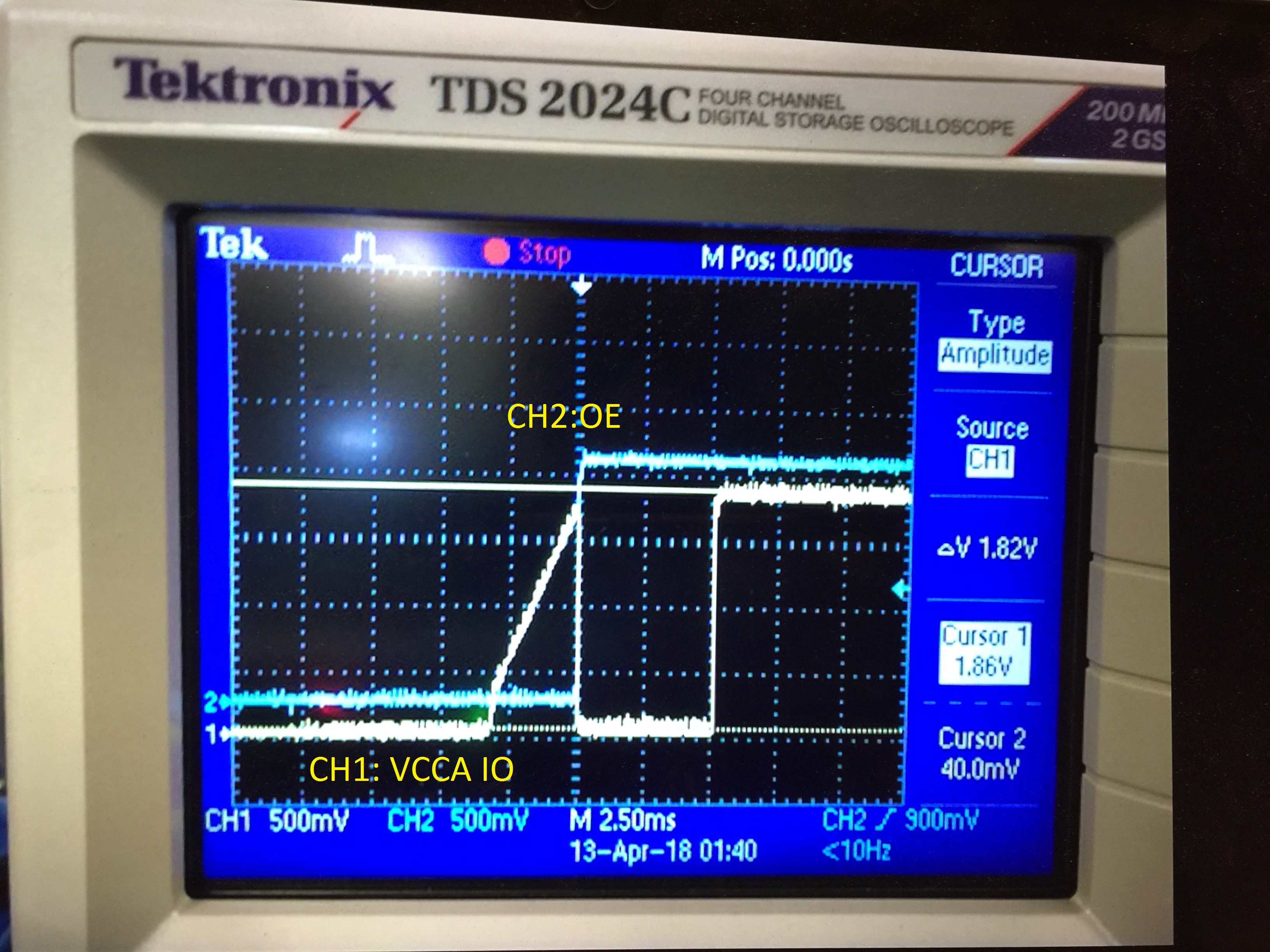
We captured glitch from the VCCA IO side when OE is enabled.

Condition:

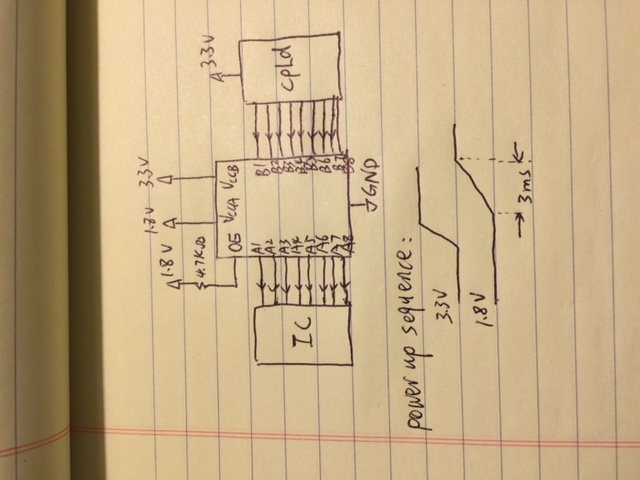
1. VCCA is 1.8V, OE is pulled up to 1.8V through 4.7K; VCCA IO is connected to IC IO with 1.8V tolerance;

2. VCCB is 3.3V, all VCCB IO are connected to CPLD IO with 3.3V tolerance;

3. VCCB 3.3V come up first;

4. 1.8V and OE come up with slew rate 1.8V/3ms. 

5. When OE come up, there is glitch up to 520mV with 1ms duration.

Can you help analyze what caused the glitch and solution to fix it?

Thanks,

-Wei


  • Hi Wei,
    Can you provide scope shots of the input/output during the glitch, and a schematic showing what is all connected to the I/O pins?
  • Hi Emrys,

    Thanks for your reply.

    The glitch waveform and schematic are shown below. 

    The glitch is from VCCA IO side, during the glitch time, the VCCB IO side is driving 0 volt by the CPLD.

  • Hi Wei,

    The shown operation is what I would expect to see during startup if the OE pin is not pulled low.

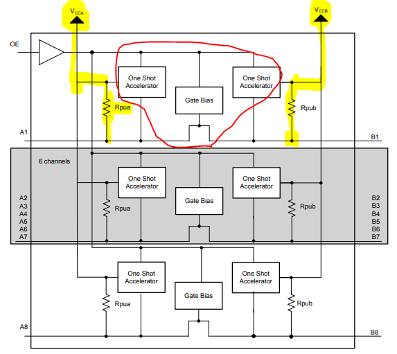
    Here's a high level block diagram of the TXS device:

    When the supply is at 0V, the device is in "Ioff" mode, which means that all inputs are in a high impedance state, and the pull-up resistors (highlighted in yellow) are disabled.  Once the supply rises above 0V, the I/O pins are no longer in a high impedance state, and the pull-up resistors will cause the voltage at the pins to rise to the supply.

    After the supply gets high enough to power on the internal logic of the device, highlighted in yellow, the pin can be driven low again.

    Note that we recommend holding OE low during startup. From section 11 of the datasheet:

    To ensure the high-impedance state of the outputs during power up or power down, the OE input pin must be tied to GND through a pull-down resistor and must not be enabled until VCCA and VCCB are fully ramped and stable.

  • Hi Emrys,

    Thanks for your reply.

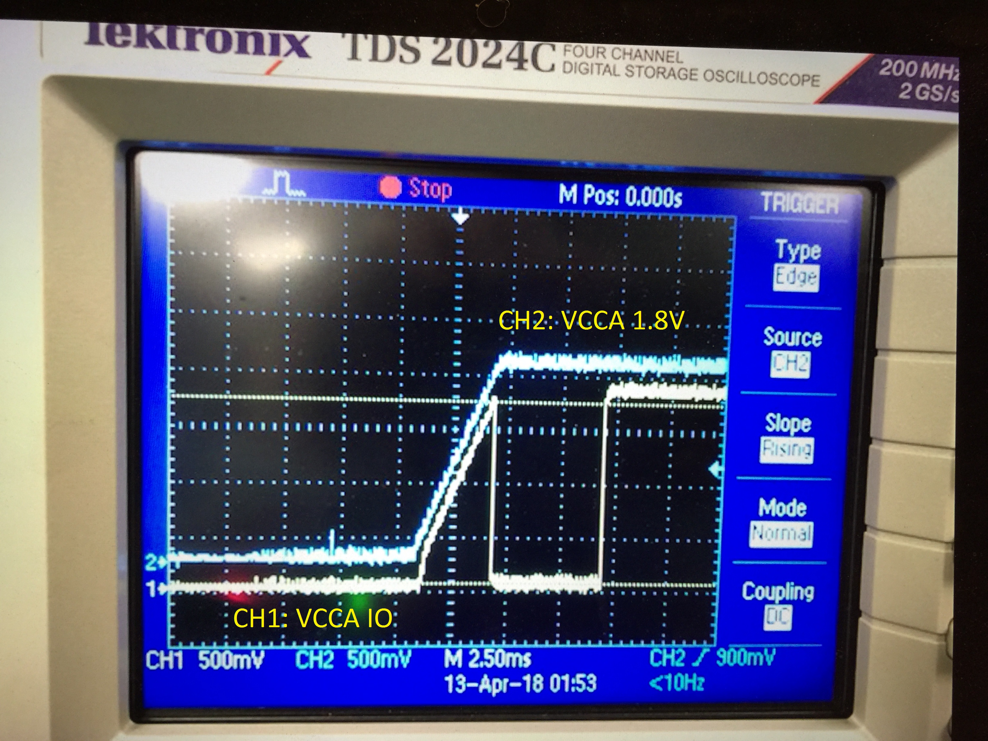
    We follow the guidance to drive OE low until VCCA 1.8V is valid, but the glitch is even worse up to 1.8V. Before it is 520mV.

    Below are the 2 waveforms between VCCA 1.8V and VCCA IO; OE and VCCA IO.

    Can you help check why the glitch is worse? Is it related to VCCA 1.8V slow rise time (3ms)?

    Thanks,

    -Wei

  • Hi Wei,
    I have asked our translation expert to look at this case to see if I am incorrect. From your test data, it seems that the pull-ups are not disconnected by OE as I had previously thought.
  • Wei Liu,

    OE pin disconnects the pullup resistors to the IO ports. The scopeshots sent seems that the device has a glitch on power ramp up.
    What is status of Vccb? Is it already stable or ramping up along with Vcca or off?
    Is there a possiblity to try powering up Vcca first and then Vccb(if its not done already)
    Also, if the inputs are floating, try having a very weak pulldown(100K) to ensure low during power ramp up.
  • Hi Shreyas,
    The VCCb 3.3V is already stable before VCCa ramp up.
    From the board power up sequence, the VCCb 3.3V is the first power rail to power up.
    So VCCa has to power up after VCCb.
    The VCCa IO side is point to point connection to the IC, it is hard to solder weak pulldown 100k to drive VCCa IO down.
    There is no internal pull up resistor to 1.8V (shared with VCCa) in the IC, the glitch ramp up the same time and same rise time as VCCa 1.8V. The only way seems still come from the TSX0108E voltage translator.
    Can you confirm?
    Thanks,
    -Wei
  • Hi Shreyas,

    We did 3 experiments:

    1. drive OE always low (0V), the VCCA IO pins ramp up together with VCCA 1.8V and stay high to be 1.8V.
    This means OE low does NOT disable the internal pull up resistor. But pull up through 40k or 4Kohm? See the 2nd experiment.

    2. drive OE pin low until VCCA 1.8V ramp up, and add 4.7k ohm pull down resistor for VCCA IO pins, the glitch ramp up the same time as VCCA but reduce to be 0.2V. This means when OE is driving low, the internal 40K ohm is enabled, therefore, through the voltage divider:
    1.8V * 4.7K/ (40K + 4.7K) = 0.19V.

    3. drive OE pin high after VCCA 1.8V, the VCCA IO voltage become 1V. This is also caused by the voltage divider:
    1.8V * 4.7K/ (4K + 4.7K) = 0.97V.

    The experiment shows the data sheet page 18 " RPUA and RPUB are disabled when OE = Low" need to further verify.

    Can you help verify on your side and let us know your feedback?

    Thanks,
    -Wei
  • Hi Wei,

    Thank you for the additional info provided.
    1) Will you confirm that once the Vcca supply is up and stable, changing the OE from high to low ( disable the IO ports), will this also cause the IO ports to be high through the pull-ups?
    2) Is the io ports high even after the Vcca supply has ramped up while the OE pin is low?

    I am trying to figure out if this is a momentary glitch during startup or if it is always like this during normal operation.
    I also look at the datasheet electrical spec w.r.t IOZ, where the IO port current is measured when OE is disabled and the max across temp being 2uA suggests that the pull-up resistor is disconnected.

    Meanwhile, I will check back with our designers to confirm the OE operation as well.
  • Did a quick check in the lab and have attached the scope shots here.

    Setup:

    Vcca = 1.8V

    Vccb= 3.3V

    B1= 3.3V , 1Mhz signal

    A1= Measure on scope

    First one with OE enabled(high), measuring Ax(A5) pin to confirm that it is pulled up to Vcca.

    The second one is with OE disabled(low), measuring A1 pin to confirm it is hi-z with internal pullup not connected

    Third is OE high, measuring on A1 pin to see the B1 signal 0 -3.3V signal translated to 0 - 1.8V signal.