This thread has been locked.

If you have a related question, please click the "Ask a related question" button in the top right corner. The newly created question will be automatically linked to this question.

LSF0108: IBIS model issue

Part Number: LSF0108
Other Parts Discussed in Thread: LSF0101

I am using LSF0108 for uni-directional translation from 3.3V (A-side) to 5V (B-side). While doing SI analysis in Hyperlynx, when I assign the IBIS model to the B-side pin, it does not give an option to assign it as an output since the IBIS of LSF0108 does not model the output. And the output at B-side always remain low, regardless of the input at A-side. I tried to define the output model in IBIS file by looking up output model parameters from datasheet and copying I-V and V-t data of I/O model, but it still didn't work and the output always remain pulled low. At A-side D-latch's (Part#: IDT74ALVCH162373) outputs are interfaced.  May I please know if something is wrong with my circuit or the IBIS model?

  •  Hi Sarmad,

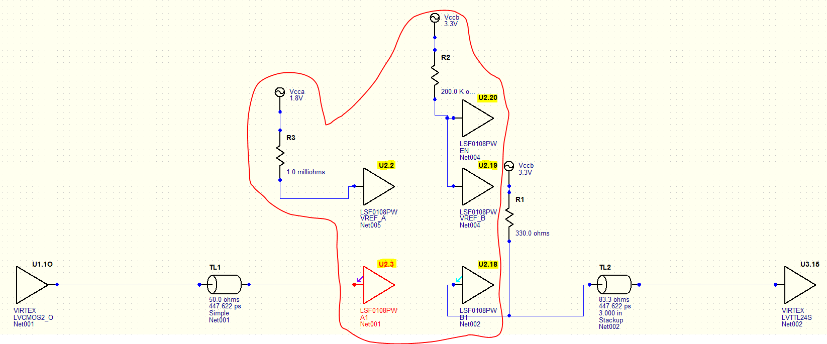
    The LSF translator isn't an active device, so you can't use it as a signal source. Here's an example showing the required circuitry (circled in red):

  • I guess I am doing exactly like that with B-side outputs pulled up to 5V. I have tried with and without pull up resistors on A-side inputs but it doesn't work in  either case.

  • What program are you using to do the simulation? Perhaps you can post the simulation file?
  • I am doing Signal Integrity analysis of the layout using Hyperlynx. Attached is the .HYP file.Digital_data_distribution_board.rar

  • Hi Sarmad,
    The board file appears to be just that -- I don't see any simulation setup or associated models in the file. Do you have a simulation file you can share like the one shown above in my post?
  • I am sharing the schematic model (.ffs) of my circuit. Hopefully this will do.

    Relay_board.rar

  • Hi Sarmad,

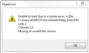
    I'm afraid that I can't get that to open with my version of Hyperlynx:

    I will ask our IBIS modelling team to look at this thread and see if they can help.

  • Hi Sarmad,

    I don't have HyperLynx so I cannot tell how your schematic looks like. Nevertheless, it should not look like the screenshot above.

    For regular buffer models (input, output, I/O, 3-state, etc), you place the corresponding symbol into your schematic and connect a net to the pin, assign the model and simulate.

    For switches, you need to place a different symbol that has 2 pins instead of 1 pin. Assign the model to this symbol (probably called switch or something like that), then specify which channel (switch) you want to use. The schematic editor should provide a GUI for you to do that, using the information in the IBIS file:

    [Series Pin Mapping] pin_2 model_name function_table_group

    3 18 LSF0101_IO_25_S 1

    According to the datasheet, on the LSF0108, pin 3 is A1, pin 18 is B1 and they are connected internally with a switch. You will tell the editor that you want to simulate this switch by selecting these pins for this symbol. Next you will wire 2 nets to this symbol, one from a driver and one to a receiver, then run your simulation.

    Bottom line is, B1 is not a driver and you won't be able to assign a output buffer model to it.

    Regards,
    JC

  • Actually I drew the circuit's schematic and layout in Altium and for SI analysis am using Hyperlynx by importing the layout from Altium. I directly assign the IBIS models to the layout pins and try to simulate it. I am using the VLS to convert 3.3V signals (A-side) to 5V signals (B-side), but it does not let me choose different voltage levels. If I select voltage level for one side the other side is automatically assigned the same level.

    Other issue that I observed is that when I try to simulate for SI analysis in Hyperlynx boardsim, it gives me an error stating that "pins u1-3 and u1-18 are associated pins according to the IBIS model". 

    And when I export the same design to Linesim and try to simulate, it does not give any error but the output on B side seems to be clamped to half the voltage level selected (1.5V in case of 3.3V level). Interestingly whatever model I select the input and output levels remain the same .i.e. 3.3V and 1.5V respectively. Although I have pulled up the signals on the B-side to 5V.

    The different responses to the same design's schematic and layout are really confusing. Kindly guide me how can I fix it?

  • Hi Sarmad,

    We are still researching this topic. Based on what we know now, it is possible that what you are trying to achieve is beyond what IBIS can offer.

    Would you mind posting a screenshot of how you hookup the VLS in Altium? We may not be able to verify with simulation but it'll help us understand the situation a little better.

    Thanks,
    JC

  • Hi Sarmad,

    We have not received a response from you in a while. We assume that somehow you are able resolve the challenges that you have. We're going to close this post for now. But if you want to follow up on this discussion, as JC alluded on the previous post, please provide him with what he asked for so that he can assist you further.

    Herman