This thread has been locked.

If you have a related question, please click the "Ask a related question" button in the top right corner. The newly created question will be automatically linked to this question.

SN74LVC2G125: Pin marking and Logic Level

Part Number: SN74LVC2G125

Hi,

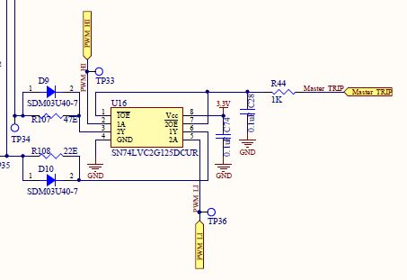
 Need to know how to identify pin1 of the device. I am using SN74LVC2G125DCUR - VSSOP (8 pin package).

 I see white line marking on one side whereas in the datasheet the index area is marked on one quadrant. Help me identify the pin1. Attaching image of layout for reference.

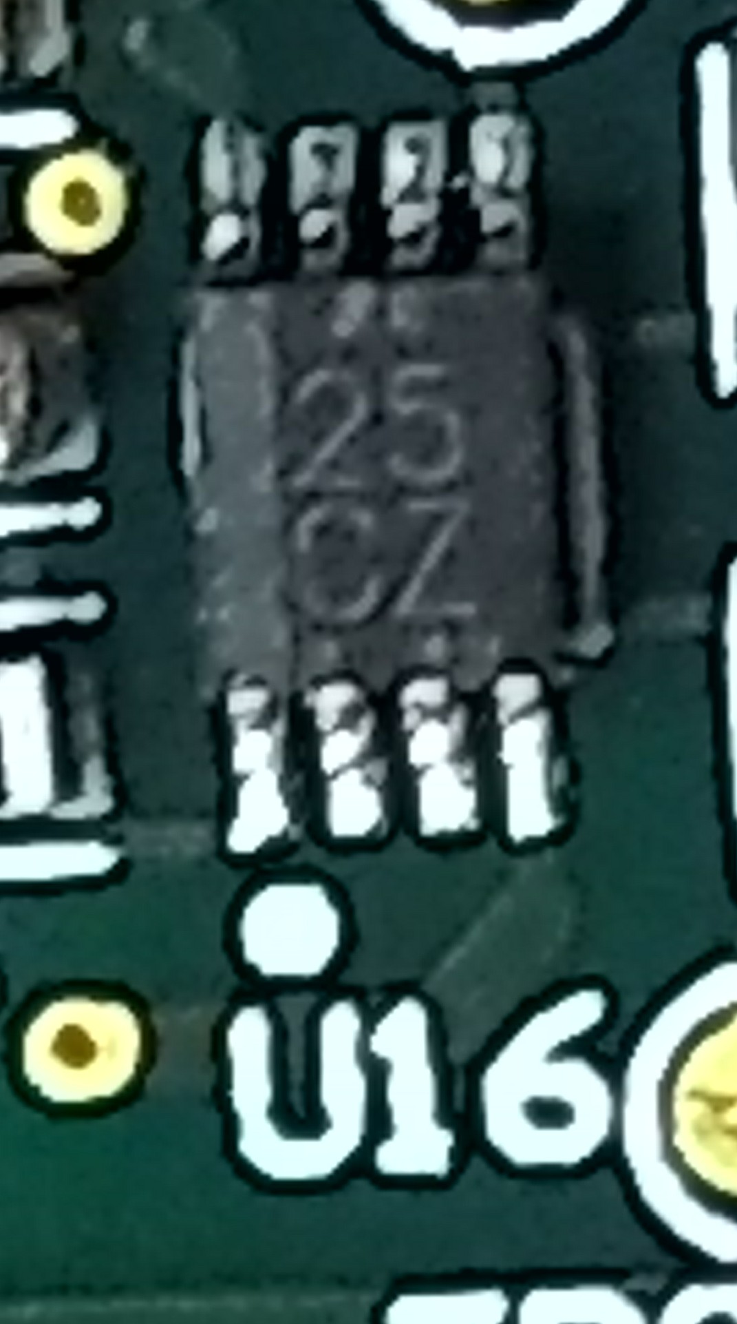
I need to have pin 1 near the white dot. Is this layout correct.

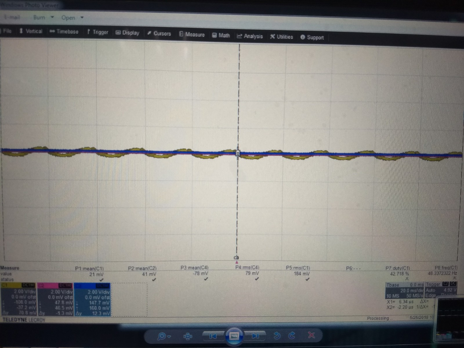
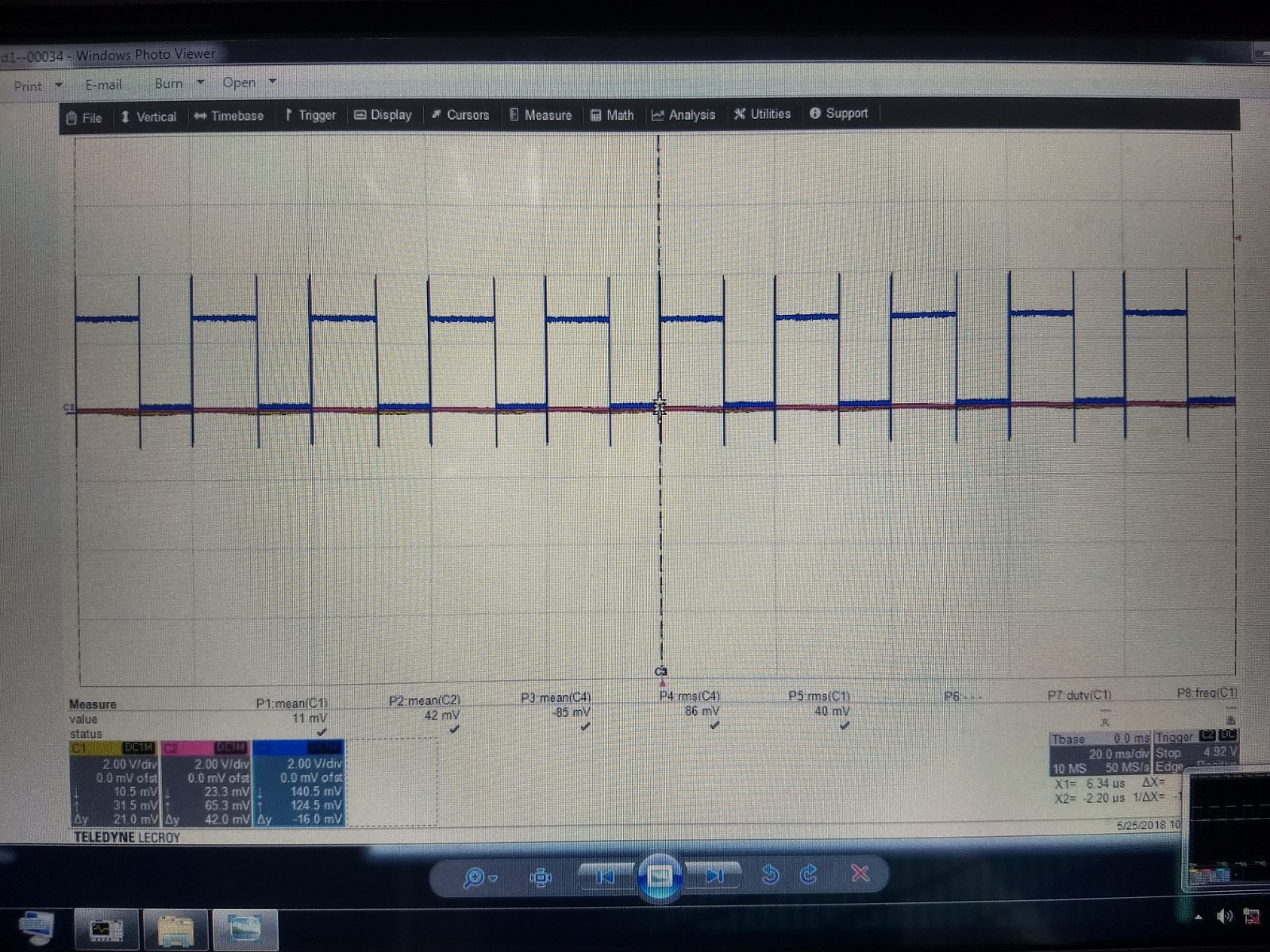
Also as per the datasheet when _OE is Low i.e 0V, the Output should be same as input. But in my device I am seeing it in reverse fashion. Why is it so?

Thanks and Regards

Arjun P Raj

  • Hi Arjun,
    In your picture above, pin 1 is at the bottom left. The dot is positioned correctly.

    Can you show me a scope shot of the input, OE, and output pins (together)?
  • Hi,

    Previously when i was testing, I was using a single probe and had found that, input and OE were at 0V and Output at Vcc Volts.

    This time i used 3 probes and tried capturing waveforms simultaneoulsy. Then the Output was not High.

    Here CH1_yellow= Input 2A(pin5), CH2_red=2OE (pin7), CH3_blue) =2Y (pin 3).


    But when I removed the probe from Input Pin5, and left that pin floating, i got Output high for 10ms, is it because of noise due to supply frequency.

    How can I eliminate this unwanted output?

    If I connect a pull down resistor at the input pins (pin 2 and 5), Will this effect be eliminated and will i be able to ensure 0V at the output.

    Thanks and Regards

    Arjun 

  • Leaving a CMOS input floating can result in many unwanted behaviors.

    All inputs should be held at a valid level at all times -- a pull-down resistor is one method to achieve this.