This thread has been locked.

If you have a related question, please click the "Ask a related question" button in the top right corner. The newly created question will be automatically linked to this question.

SN74LVC3G17: DSBGA pinout unclear from datasheet

Part Number: SN74LVC3G17
Other Parts Discussed in Thread: TS5A3359

Hi,

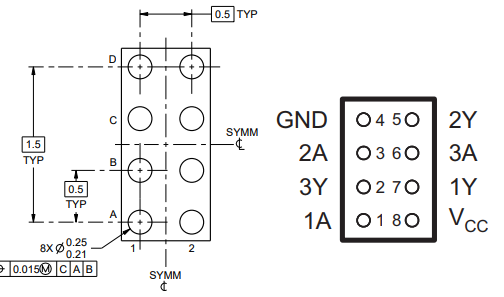
I'm creating the footprint for this part and I have difficulty making sure of the right pinout.

In the recommended footprint, the balls are numbered as:

A1    A2

B1    B2

C1    C2

D1    D2

But in the "Pin Configuration and Functions" section, the pins are numbered as:

Bottom View

4    5

3    6

2    7

1    8


I'm pretty sure that pins 5, 4 = A1, A2, 6,3 = B1, B2, etc., but I would like to be sure.

Thank you,

Fred

  • Hey Fred,

    So pins 1, 8 = A1, A2 and pins 2,7 = B1, B2. Sorry for the confusing pin layout in the datasheet.

    Here is a picture of this package from bottom view right next to each other.

    It is really easy to see from this diagram of the package from bottom view that pin A1 is equal to pin 1.

    Thanks!

    - Karan

  • Thank you, that answers my question.

    It is indeed clear, but it's always better to be sure I guess.

    Maybe it'd be worth it to adjust the datasheet? If I compare datasheet of the TS5A3359, which has the same package as the SN74LCV3G17, the pinout table leaves no place for doubt by addressing the pins as A1, A2, etc., which is the same denomination as the recommended footprint.

    TS5A3359

    Thank you,

    Fred