This thread has been locked.

If you have a related question, please click the "Ask a related question" button in the top right corner. The newly created question will be automatically linked to this question.

TXB0304: Push pull does not work with CMOS logic from 1.8V to 3.3V

Part Number: TXB0304
Other Parts Discussed in Thread: TAS5754M, SN74AVC4T774

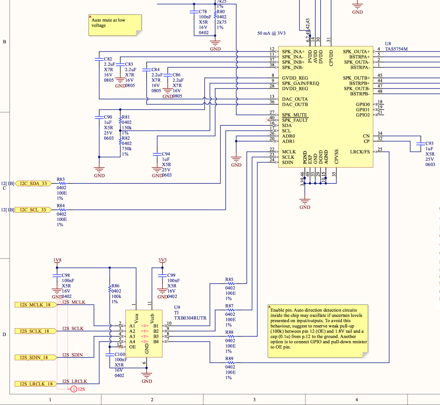
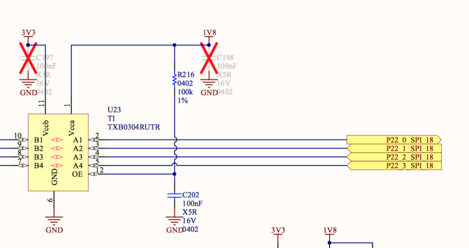
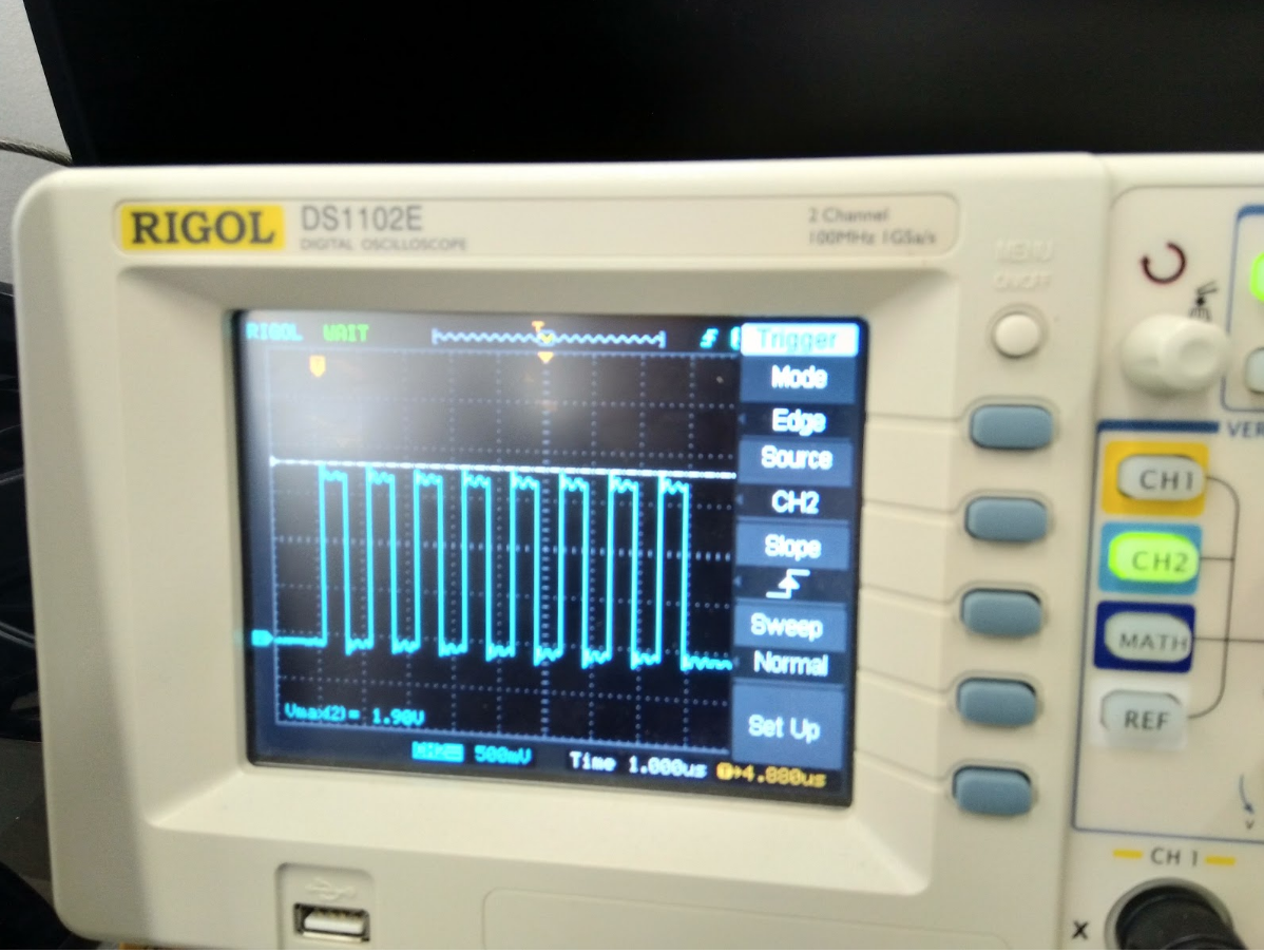
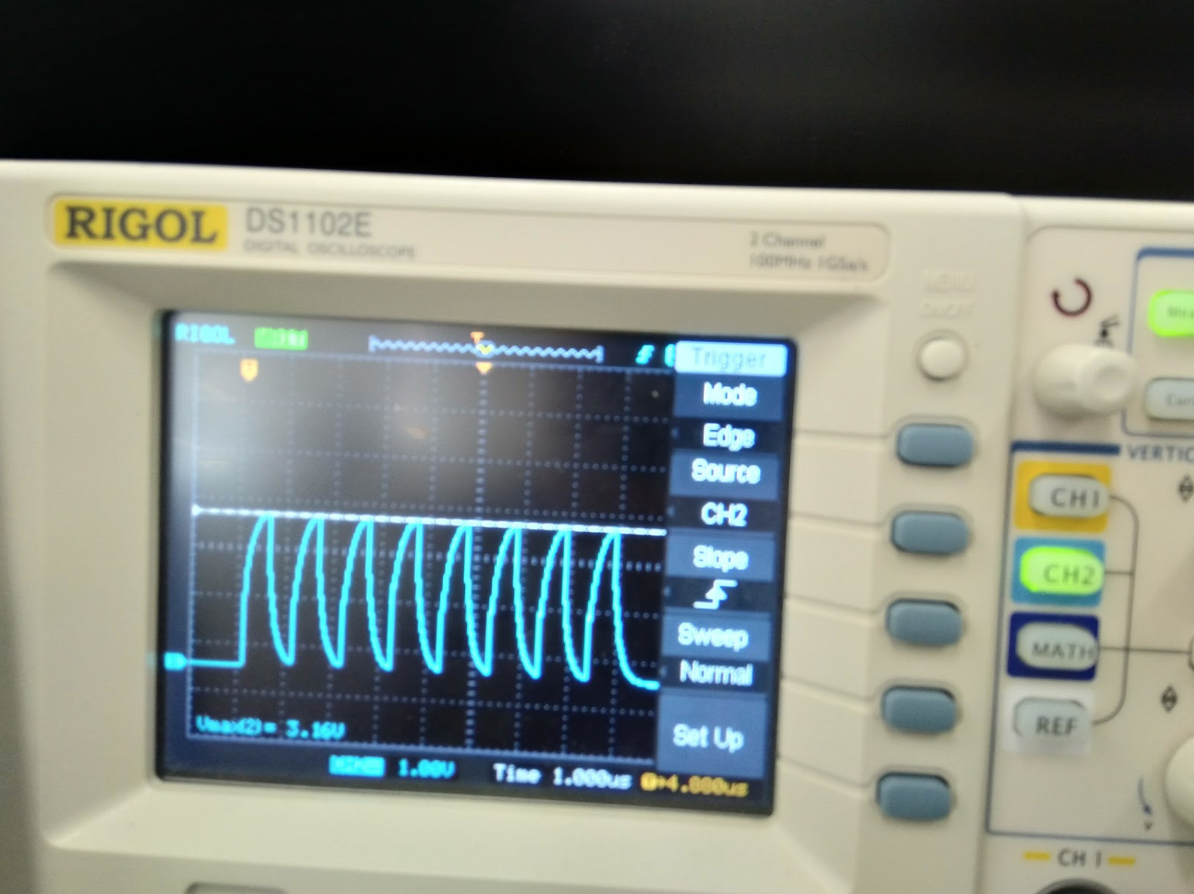
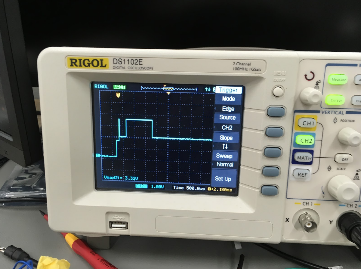
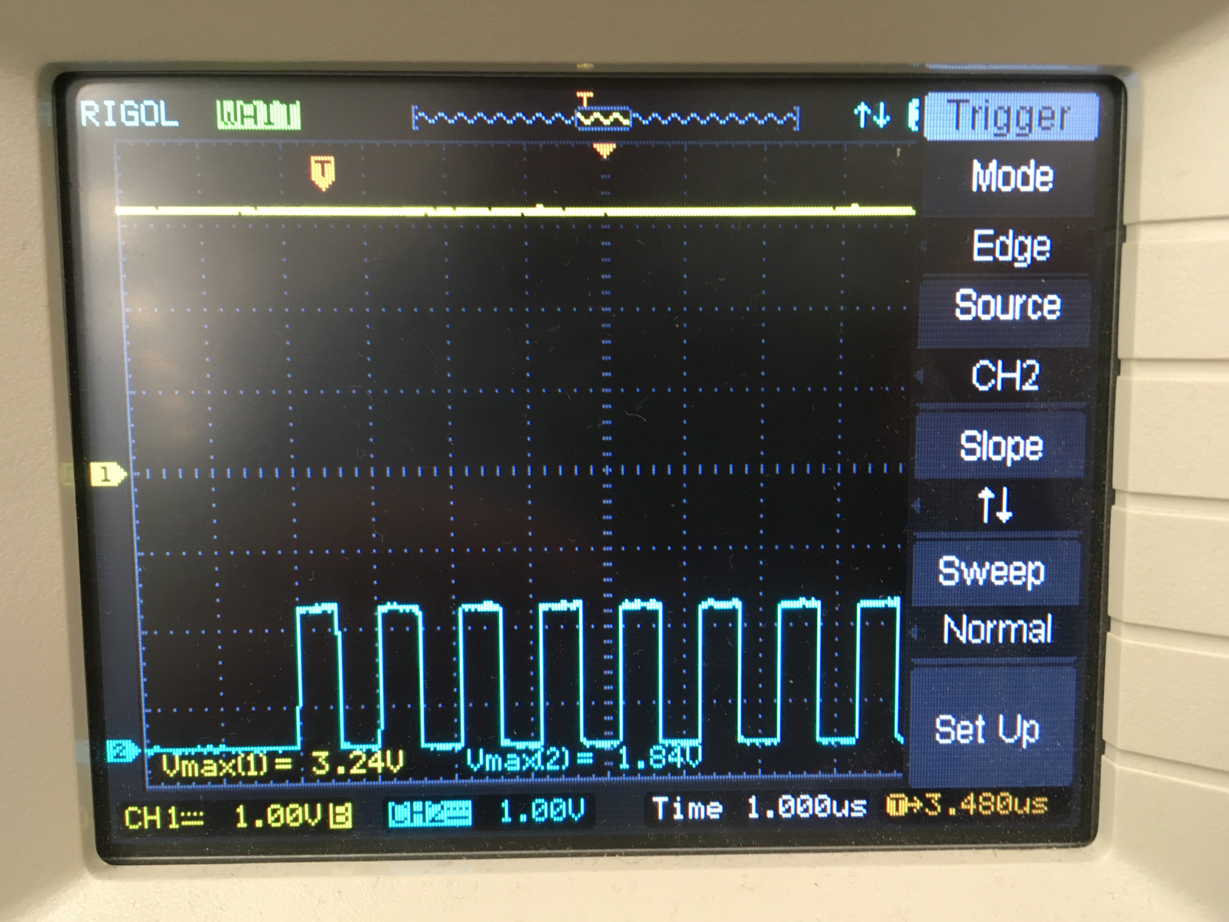
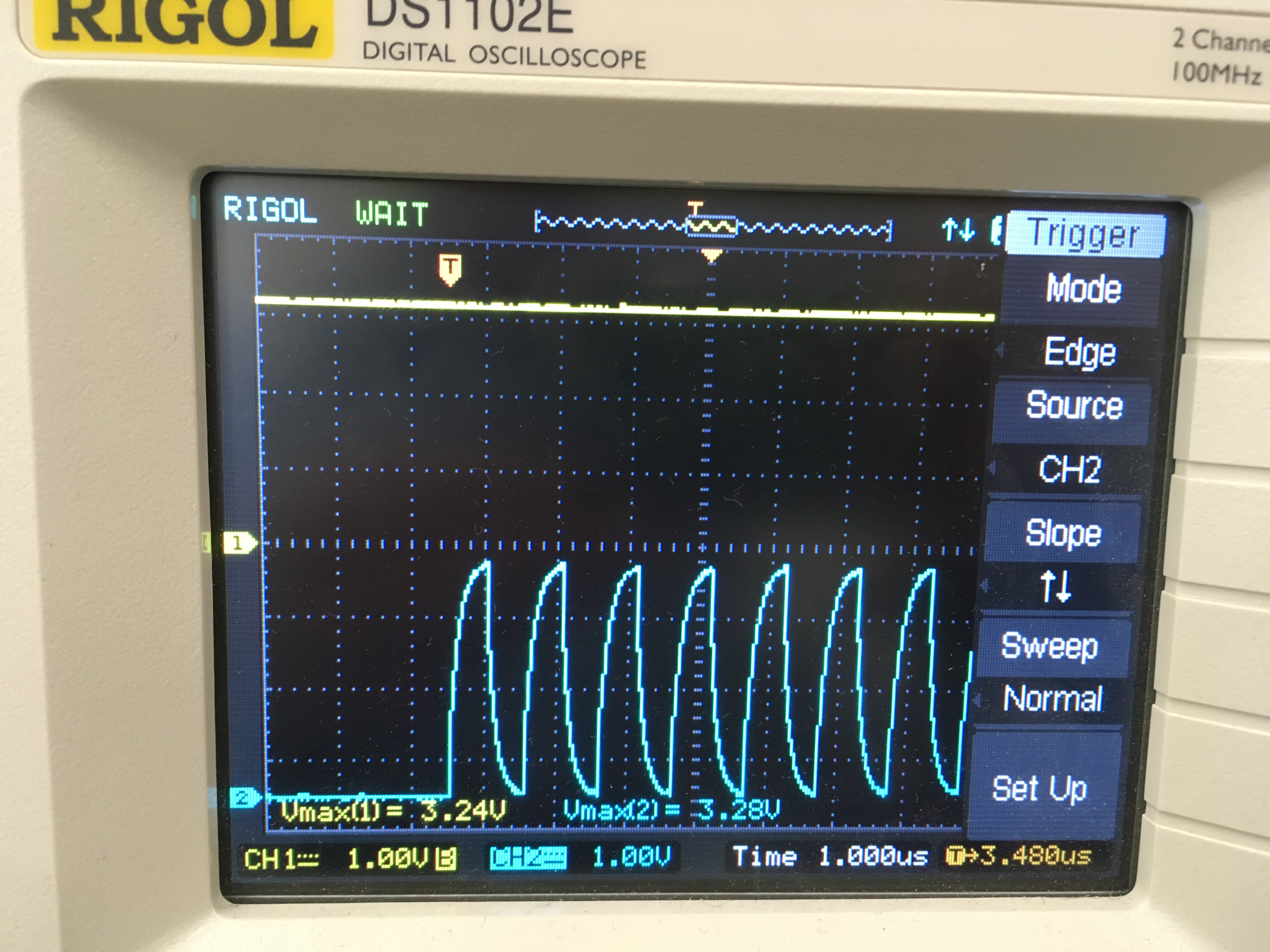
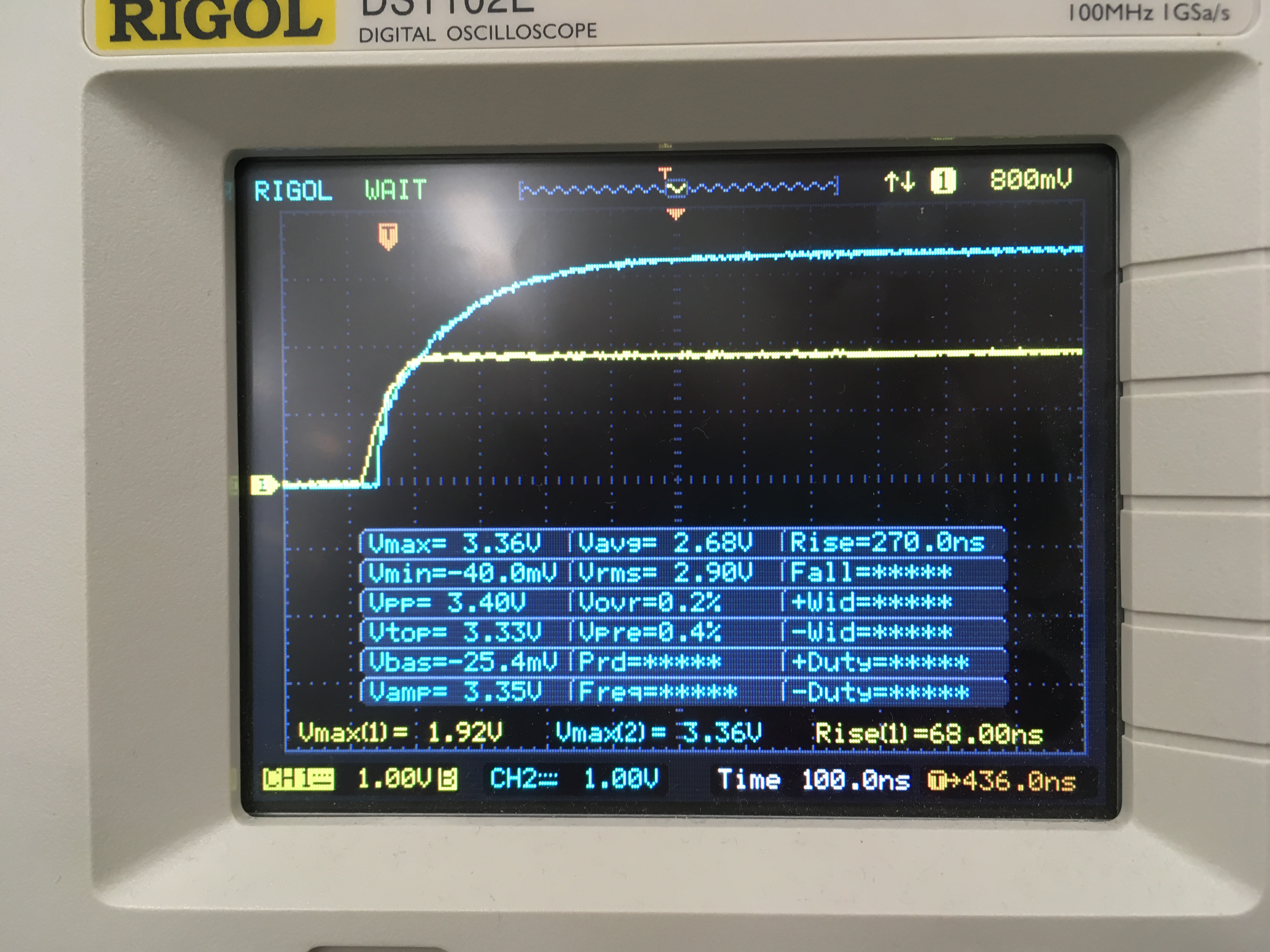
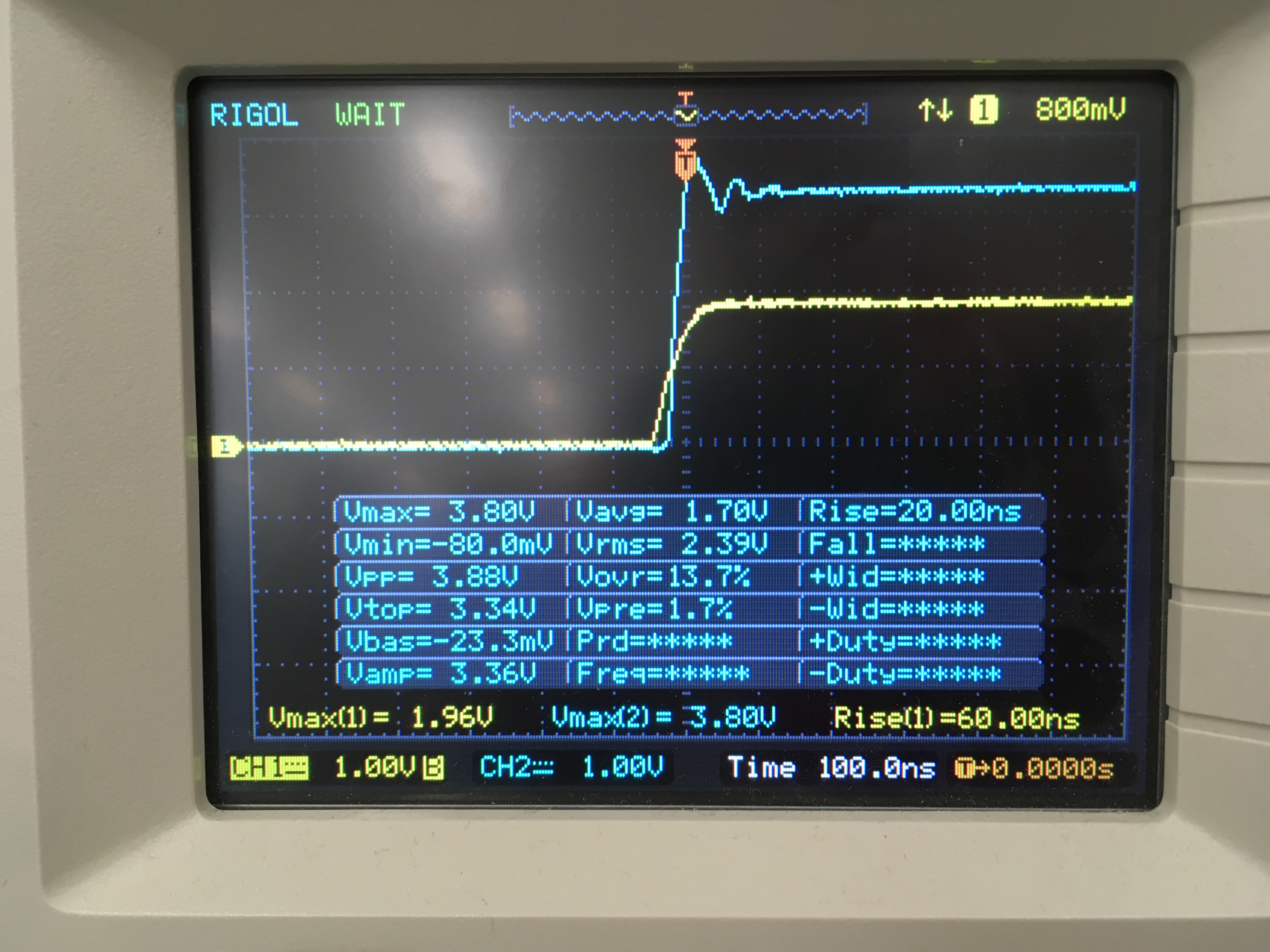
A customer of mine is using the txb0304 with on one side 1.8V and 3.3V that is not working. No open drain, but push-pull logic. The only way the level shifter is working is by using a 10 kΩ pull-down in the form of a cable on the output. Can you help to solve this issue?

  • Please see below for the schematic. It is used in two places on the board, having troubles in both cases.

    Case #1: level shifter for I2S signals from Qualcomm Snapdragon to TI TAS5754M. There is a nice clock signal of 1.8V coming from the Snapdragon, but no signal on the output towards TAS5754M.

    Case #2: 

    Left-hand side goes to a connector with a short cable to the board that uses 3.3V CMOS logic. Right-hand side goes directly to the same Qualcomm Snapdragon pins.

    In one setup, adding a 10 kΩ pull-down on B1 helped solve an issue where it varied the signal on A1 between 3.3V high level and 1.8V low level. After adding the pull-down, low level was 0V and signal was read correctly. Could not be reproduced on a second board with a different cable.

  • Hi Martijn,

    I will have our translation expert take a look into this when they get into the office tomorrow. Could we get some scope shots of the input, output, and both VCC rails to better help us debug this issue. Also, the schematic for case 1 looks like there is a no connect symbol on the OE pin. Is it possible that it wasn't routed in the layout? If the OE pin is floating this could be the reason the outputs aren't working.
  • Dear Dylan,

    Thank you for looking into this! I checked the PCB, I confirm the OE pin is in fact routed properly on the board and pull up to the 1.8V rail, I don't know what the no connect symbol is doing there.

    For Case #2:

    Clock signal 1.8V before level shifter (pin A4)

    Clock signal 3.3V after level shifter (pin B4) (presence of cables on the connector does not affect the shark fin shape):

    Incoming data signal 3.3V side (pin A2) (note that the low level is not 0V as expected but 1.8V)

    To solve the latter, a 10 kΩ pull-down was added on the 3.3V board, this pulled down the logical low level to 0V and things work properly. This same fix does not work, however, when another cable is used.

    Thanks.

  • Hi Martijn,

    Thank you for the schematic and the scopeshots.

    On the schematic, you have noted that the OE pin needs to have pullup resistor and capacitor 100nF. I would not suggest using the capacitor on the OE pin. this RC causes slow rising edge on OE pin which is not good for the CMOS device.

    on the post, you have mentioned that the A2 signal is 3.3V, whereas the Vcca port supply is at 1.8V, why is that? 

    I would not suggest using a pullup or pulldown on the TXB010x or the TXB030x devices, and not such a strong resistor especially. The reason is that there is internal series 1K resistor on the TXB device which forms a voltage divider at the output. Please refer to the app note regarding this 

    finally, there is another requirement for the TXB030x device to have the driver strength of at least 3mA to sink or source current in order to change(overdrive) the signal levels, as mentioned in the datasheet. Does the Qualcomm chip provide this drive strength?

  • The shark fin shape also indicates to me that the output loading is large. do you know the scope probe capacitive loading. Are you using a passive or active probe?
    an SMB probe can have cap loading of at least 100pF + the board traces + input loading at the scope will be additional loading on the device.
    If its possible, please measure the output of the TXB device at the pin disconnecting the TI TAS5754 device and the series 100ohm resistors as well.
  • Dear ShreyasRao,

    Thanks for helping out.

    [SR]>> On the schematic, you have noted that the OE pin needs to have pull-up resistor and capacitor 100nF. I would not suggest using the capacitor on the OE pin. this RC causes slow rising edge on OE pin which is not good for the CMOS device.

    Thanks for this suggestion, I will try this out.

    [SR]>> on the post, you have mentioned that the A2 signal is 3.3V, whereas the Vcca port supply is at 1.8V, why is that? 

    Sorry, mistake on my part, I meant B2. I checked this also on the PCB to be sure. So Vcca is 1.8V and A side is 1.8V, B side is 3.3V (in both cases).

    [SR]>> I would not suggest using a pullup or pulldown on the TXB010x or the TXB030x devices, and not such a strong resistor especially. The reason is that there is internal series 1K resistor on the TXB device which forms a voltage divider at the output. Please refer to the app note regarding this 

    Thanks for sharing the application note. This led me to thinking about the other end of the clock signal for case #2, which also has a 100Ω series resistor. I don't know how the designer of the board came up with that value, but could it be that this is causing issues as well, and what would be a better value?

    [SR]>> finally, there is another requirement for the TXB030x device to have the driver strength of at least 3mA to sink or source current in order to change(overdrive) the signal levels, as mentioned in the datasheet. Does the Qualcomm chip provide this drive strength?

    Yes it is configurable between 2 and 16 mA, and currently it is set to 12 mA.

    [SR]>> The shark fin shape also indicates to me that the output loading is large. do you know the scope probe capacitive loading. Are you using a passive or active probe? 
    an SMB probe can have cap loading of at least 100pF + the board traces + input loading at the scope will be additional loading on the device.

    I am using a passive probe. 

    [SR]>> If its possible, please measure the output of the TXB device at the pin disconnecting the TI TAS5754 device and the series 100ohm resistors as well.

    I will try as soon as possible.

    Thanks.
    Martijn

  • Hi Martjin,

    Thanks and please let me know if you have any update on this.
    I have this post tracked so once you reply, I will be notified.
    I will be curious to know about the results and the final fix for this.
  • I have removed the capacitor on the OE pin: no change.

    I also removed the pull-downs and disconnected the cable to the other board.

    What you see is this as input to the level shifter:

    And the output is this, without anything attached at the output, e.g. no pull-ups/pull-downs, capacitors or series resistors:


    The voltage rails on 1.8V and 3.3V show a straight line, no glitches at all.

    Drive strength of the Snapdragon is set to 12 mA.

  • Martjin,

    Drive strength of the incoming signal is good.
    The shark fin shape represents loading at the output.
    Do you have an active probe to measure the output at the pin? Passive probes can have higher load capacitance combined with the input cap of the scope itself.
    Do you still see the strange waveform (third one) seen in the earlier post?
  • Martjin,

    Is there any further update on this or should i close this?
  • We don't have an active probe to test with.

    Will try next week with the SN74AVC4T774 that we just got in, hopefully that will work better.

  • I created a measurement setup with the TXB0304 EVM and a home-made SN74AVC4T774 EVM. No pull-ups/pull-downs are present. Both devices are connected in the same way to the Qualcomm Snapdragon development kit. The 3.3V output is unloaded in both cases, just measuring with the oscilloscope.

    These are the results:

    Step function with TXB0304 (yellow = 1.8V input, blue = 3.3V output):

    Step function with SN74AVC4T774 (yellow = 1.8V input, blue = 3.3V output):

  • Hi Martjin,

    I believe the performance of the AVC4T774 is much better as compared to the TXB, as expected.

    Please let me know what you think and if AVC4T774 will be your device choice.

  • As a next step I am looking into patching my PCB, replacing the TXB0304 with the AVC4T774, then see how it performs in the wild.
  • Please keep me posted on the results. I strongly beleive that the SN74AVC4T774 should be the fix.
  • The board has been patched where the TXB0304 has been replaced by the SN74AVC4T774 using an adapter PCB.

    The clock signal, which is generated at 1.8V and has to be shifted to 3.3V, looks like this now (yellow line) (this used to be the sharkfin-shaped signal):

    The signal is crisp, and the ringing is correlated with the power supply, so we will have to add a capacitor near the level shifter power supply input near the IC (not done currently).

    Shifting the other way, from 3.3V to 1.8V level:

    So the level shifter also seems to work properly in this direction.

    Based on this I would say that the TXB0304 is not suitable for my application and that the answer is to use the SN74AVC4T774 instead. Thanks all for the support.

  • Martjin,

    The TXB devices are auto bidirectional devices without much drive strength and usually suited for high impedance loads.

    It seems that the loading on the output was beyond the TXB capability and I am glad that the actively driven AVC4T774 was able to resolve this.

    let me know if anything else.

  • Unfortunately, I was not able to view the scopeshots which you had attached in the post. but I believe that sharkfin shaped waveforms are now much improved.