This thread has been locked.

If you have a related question, please click the "Ask a related question" button in the top right corner. The newly created question will be automatically linked to this question.

TXS0108E: Level Translation Problem

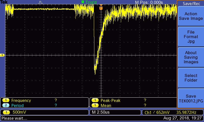
Part Number: TXS0108E

Hi,

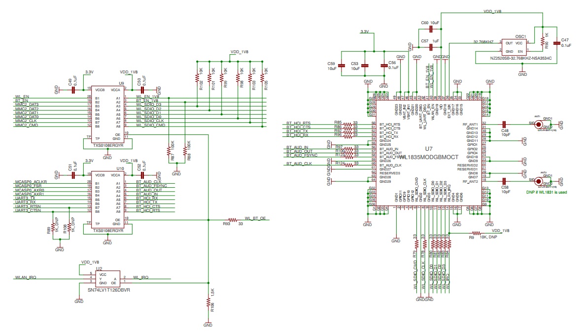
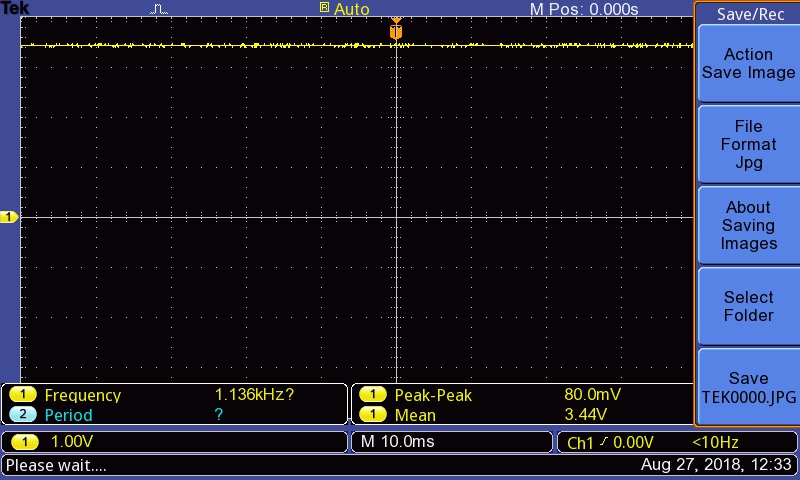
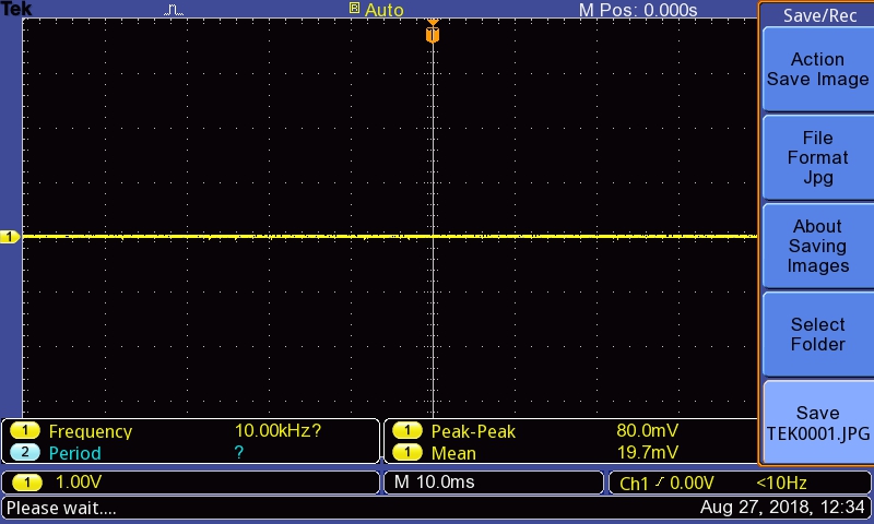
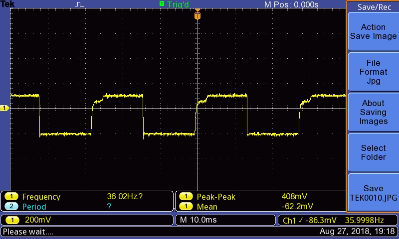
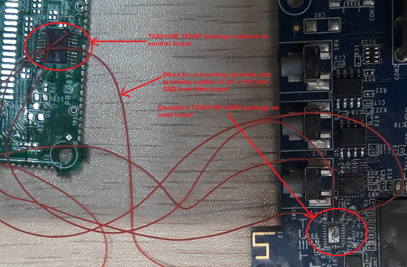
We are facing issue with the Level translation in TXS0108ERGYR IC. We are providing logic 1 (+3.3V) to one of the B channel pin(B1), we should get logic 1 (+1.8V) on corresponding A channel pin(A1) but unable to get it. Attached is the image showing the same of our our application. 

Please let us know the whether we need to any other changes.

  • We are getting logic 0 (0V) on corresponding A channel pin(A1).
  • Hi Kamesh,
    Can you provide an oscilloscope shot of the input and output signals?
  • Hi Emrys Maier,

    Thank you for  the reply. Please find the attached images for the oscilloscope shots. Name of oscilloscope shot/image is as per the channel on which measured.

    Regards,

    Kamesh Lakhwani

  • Hi Emrys Maier,

    We have also observed below cases:

    1) When we provide a Clock signal on pin B7 from a function/signal generator, we observed below waveform on CRO. The corresponding  output on pin A7 is also shown below it. During this measurement the pull-up resistor R103 was mounted on MMC2_CLK signal on Pin A7.

    Signal on Level Translator Pin B7:

    Signal on Level Translator Pin A7:


    2) When we provide a Clock signal on pin B7 from a function/signal generator, we observed below waveform on CRO. The corresponding  output on pin A7 is also shown below it. During this measurement the pull-up resistor R103 was not mounted on MMC2_CLK signal on pin A7.

    Signal on Level Translator Pin B7:

    Signal on Level Translator Pin A7:


    Also, we are trying to understand why the level of the square wave shifts down from reference plane as observed on MMC2_CLK signal on pin A7(as shown above) when pull-up resistor R103 was not mounted.

    Please let us know this as soon as possible. Hope the above will help you understand the scenario and you can provide the required support accordingly.

    Best Regards,

    Kamesh Lakhwani

  • Hi Kamesh,

    1) Why is the input to the TXS0108 not DC offset? I see that the swing of the input signal is around zero. The input should be corrected.
    2) The TXS0108 device shown here have pullup and pulldown resistors externally. Please remove these. the TXS devices have internal pullup resistances which should be sufficient for operation.
    3) The TXS device OE is connected to gnd by default through the pulldown resistor but the OE is active high enable pin. What is the status of the WL_BT_OE pin?

    There are 2 TXS0108 devices in the schematic. Is the issue seen on both of them or only on U9 or U10?
  • Hi Mr. Shreyas,

    Thank you for your reply. 

    1) Why is the input to the TXS0108 not DC offset? I see that the swing of the input signal is around zero. The input should be corrected.

        OK I will add some offset in the signal from Function Generator. But why DC offset is required to be added ? This will not allow to shift the square wave below the reference on output..right ?

    2) The TXS0108 device shown here have pullup and pulldown resistors externally. Please remove these. the TXS devices have internal pullup resistances which should be sufficient for operation.

        Actually we have followed the beaglebone black wireless design and also have the board with us. In this board, the level translator is perfectly working even with Pull-up and Pull-down resistors. Below is the link         for the same for your reference:


    3) The TXS device OE is connected to gnd by default through the pulldown resistor but the OE is active high enable pin. What is the status of the WL_BT_OE pin?

        We have enabled the OE by pulling it high but still we are not getting the results.

    There are 2 TXS0108 devices in the schematic. Is the issue seen on both of them or only on U9 or U10?

        The issue is seen on both of them.

    Regards,

    Kamesh Lakhwani


  • Kamesh,

    The signal not having a DC offset is actually violating the abs max conditions of the device which states that the input port should not go below -0.5V.

    please see the app note on effects of pullup and pulldown resistors here below:
    www.ti.com/.../scea054a.pdf

    The Voh and vol will be affected with the strong pullup resistors in parallel with the internal resistors.
  • Hi Shreyas,

    We have removed the pull down resistor on signal WL_EN but still are not able to get the level translated.

    Regards

    Kamesh

  • Kamesh,

    Sorry I wasn't clear on the pull-down resistors. The resistors on the IO ports of the TXS device need to be removed.
    The OE can have the pull-down which needs be over driven by the WL_EN signal.
    Did you add the offset so that the signal is at gnd when low?
  • Hi Shreyas,

    I mean to say that we have removed pull down resistor R87 that is on WL_EN_1V8 signal as there are already internal pull up and pull down resistors present on chip. OE is held high and the chip enabled. But still we are not getting 1.8V level on WL_EN_1V8 line even though WL_EN is having DC 3.3V level.

    Regards

    Kamesh

  • Kamesh,

    Let me know once you have the DC offset added to the input signal.
    Please send scopeshot as well.
  • Hi Shreyas,

    Signal on WL_EN is DC of level +3.3V(Logic 1). It is not a square wave. This signal is directly the output of the Processor. Sorry, but are you trying to say that we should add offset to this signal ? How ?
    We can do one thing..We disable the processor output or put logic 0 on this signal. Apply +3.3V(Logic 1) from external source and observe the output. Also, we have done this exercise before but can't get the output from Level Translator of +1.8V level.

    Please correct me If I am wrong. Thank you for your kind support.

    Regards,
    Kamesh
  • Kamesh,

    I was not aware about this scenario as all the discussions and the scopeshots you had provided before had a square wave without any DC offset.
    The TXS device by default have the IO ports at the respective Vcc voltage levels and hence the 3.3V input should have 1.8V level on the corresponding IO port.
    in order to isolate what is causing this behavior, please try to isolate the device from the LV1T126 and the other TXS to see if the levels change; remember to have the OE enabled by connecting it to Vcca.
    Once changed, connect it back to the system to see if the device has the issue again. If the issue repeats, then the OE may not be correctly asserted
  • Hi Shreyas,

    Sorry if I was not able to explain you the scenario fully. 

    We have performed one exercise as below:

    1) Currently we are using VQFN package of the TXS0108E on our Main board(Actual customized hardware that we have made for our application). We mounted TSSOP package of TXS0108E on another board
    2) On the Main Board, we unmounted/desoldered the IC U9(ref des as per the schematic)
    3) On the Main Board, we shorted channel B1(WL_EN) pcb pad with +3.3V supply, so that we get logic 1 on this pcb pad
    4) Took wires from channel B1(pcb pad) on the Main Board and soldered it on channel B1 of the TSSOP package on another board
    5) Took wires from channel A1(pcb pad) on the Main Board and soldered it on channel A1 of the TSSOP package on another board
    6) Also, we have given supplies +3.3V, +1.8V and GND connections from our main board

    We observed that the Level was translated on the TSSOP package. That is, with logic 1(+3.3V) on channel B1 we are getting logic 1 (+1.8V) on channel A1. 

    Attached the image showing the above explanation.

    Regards,
    Kamesh

  • Hi Shreyas,

    What can be the issue here ?

    Thanks & Regards,
    Kamesh

  • Hi Kamesh,

    The fact that the TXS0108 works on one board, but not on main board indicates that the device is functional, working as expected and doesn't have issues. It may also be an indication that the main board needs to be looked at for possible defects.

    Are both the system gnd and device gnd at the same level on the main board? is there anything on the main board which is loading the output such that it is not able to maintain the 1.8v level?

  • Hi Shreyas,

    Sorry for late reply. Yes, the system gnd and device gnd are at the same level on the main board. We are thinking to solder a new level translator IC on fresh bare board.

    Regards,
    Kamesh

  • Kamesh,

    Please let me know how the fresh device on the new board works.