This thread has been locked.

If you have a related question, please click the "Ask a related question" button in the top right corner. The newly created question will be automatically linked to this question.

SN74GTL2003: SREF pin impedance

Part Number: SN74GTL2003
Other Parts Discussed in Thread: TINA-TI

Hello,

My customer is using SN74GTL2003 to translate between 3.3V and 1.2V.  The current design now needs to translate between 1.2V and 1.05V.  The data sheet says that the the GREF input must be connected to DREF and both pins pulled to HIGH-side VCC through a pullup resistor (typically 200 kΩ). But the high side (1.2V) is now connected to the S inputs.

The current plan is to rotate the chip 180 degrees which will put the 1.2V signals on the D side and 1.05V signals on the S side. The only problem is the need to supply 1.05V to the SREF pin and 1.2V is only available.  A resistor divider could be used to lower the voltage at SREF, but we don't know the input impedance of SREF pin to figure out what resistance would work. The customer is thinking of a resistance value that is low like around 100 ohms which would only dissipate about 12 mW. 

Would this resistance value work in this fashion? Do we have the impedance information for the SREF pin?

Thank you so much for your help!

Best regards,

Errol Leon

Texas Instruments

Field Applicaitons Engineer

  • Hi Errol,
    Rotating the device 180 degrees will result in the ground pin being at the D8 connection, and the gate connection (G_REF) will connect to S8. I don't think that's going to do what you want.

    Can you provide a schematic showing the connections you described above? I don't really get it from the text.
  • Hi Emrys,

    Thank you for supporting this quickly! Yes, the customer realizes some pins will not have the right connection, but will fix with some cuts and/or jumps. I have a partial schematic that I can send to you through private message.

    Thank you!
    Errol
  • Hi Errol,

    Thanks for the email.  I will also post my response here for anyone who stumbles onto this thread.

    *****

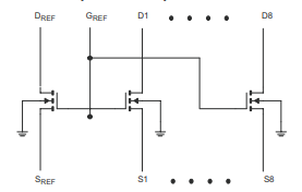
    Note first that the nFETs in the SN74GTL2003 are 4-port, meaning they have no designated Source or Drain:


    That means that when V(S1) > V(D1) then the “S1” pin becomes the drain, and the “D1” pin becomes the source.  It’s a terrible naming convention if you ask me, but it is what it is.


    The biggest issue I see for translating from 1.05 to 1.2V is that the voltage difference between 1.05 and 1.2V is only 0.15V, and is not enough to turn on the bias FET.  You need at least a 0.8V difference (preferably 0.85V, and recommended 1.0V) to get a reliable bias.


    To translate from 1.05V to 1.2V, this is how it would have to be done:


    Here you can see that the direction of translation doesn’t matter – I have channel 1 going from 1.05 (D1) up to 1.2 (S1), and channel 2 going from 1.2 (D2) down to 1.05 (S2).


    There’s a video series that explains how this works in detail if you’re interested (using the LSF family of parts as an example, but GTL2003 works on the same principle): https://training.ti.com/LogicMinute


    Also, I have attached a Tina-TI simulation of the LSF that I have used in the past.  It’s not a perfect representation of the LSF or the GTL, but it’s close enough to see the basic concepts at work.

    LSF0108_7MHz_1V2.TSC

  • Hello Emrys,

    Thank you for the detailed explanation. This was able to solve my customers issue!

    Best regards,
    Errol