This thread has been locked.

If you have a related question, please click the "Ask a related question" button in the top right corner. The newly created question will be automatically linked to this question.

SN74AVC8T245: Maximum trace length

Part Number: SN74AVC8T245
Other Parts Discussed in Thread: SN74AXC8T245

Hello,

I am Using SN74AVC8T245DGVR part in my project.

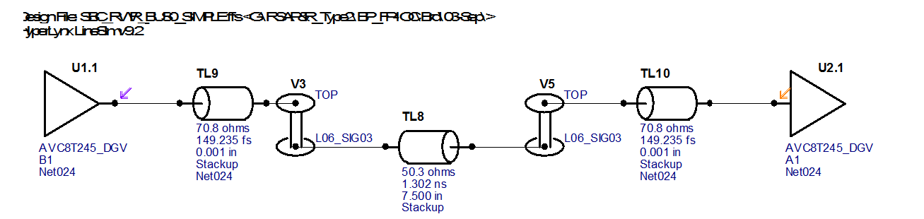
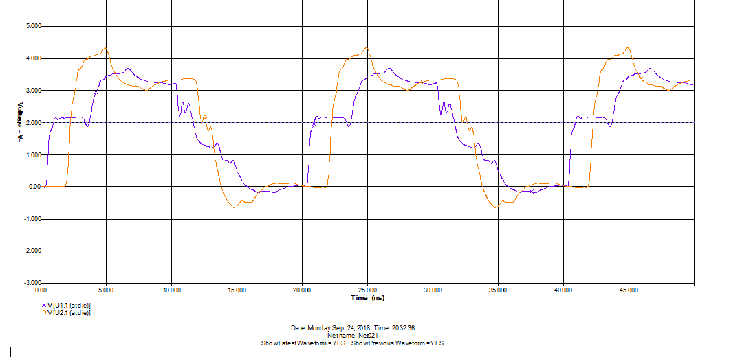
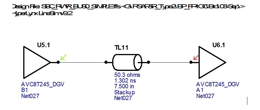
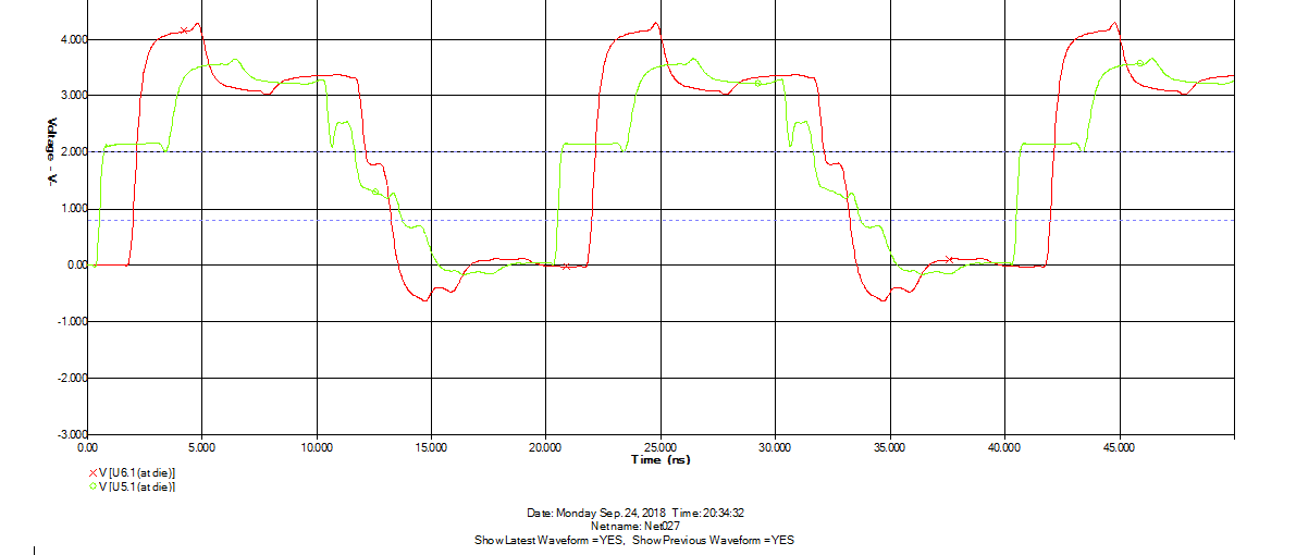
Actually this level translator output is connected to receiver section and having a trace length around 6.7 inches approx.

Operating speed will be 50 Mbps.

Can you please suggest what is the maximum trace length for this level translator?? 

Any terminations are required for this??

Regards,

Ramesh M

  • Hello Ramesh,

    There are many factors affecting trace length requirements.  These include (but are not limited to):

    • Trace length (reflections, total resistance)
    • Trace geometry (reflections)
    • Trace thickness (resistivity)
    • Trace width (capacitive load, resistance)
    • Substrate material (permittivity)
    • Nearby traces (parasitics)
    • Existence of power planes (capacitive load)

    At the length you describe, transmission line effects will begin to manifest and it will be difficult to give a reasonable signal integrity expectation without many details.

    I would recommend using a simulator to do a transient analysis of the waveform using TI's IBIS model (available here:) and your board's geometry as inputs.

    I believe this is most commonly done in one of these three software suites: HyperLynx, Advanced Design System (ADS), or Microwave Office.

  • Hi,

    Thanks for your inputs.

    Actually this buffers are the in between motherboard and daughter card(24-Bit parallel bus).

    I have simulated this buffer without including connector model by Hyperlynx9.2, Please refer below waveform at 50MHz 

    I am not getting proper waveform its peak to peak around 4.9Vp-p. The same lines i have simulated with simple one transmission line, still i am getting the similar problem,

    Please refer the below one,


    Model selected: AVCB164245_IO_33

    Can you please guide us to implement this with good signal integrity.

    Regards,

    Ramesh M

  • Hey Ramesh,
    Can you try the same simulation with the IBIS model for the SN74AXC8T245? This device was just recently released and has a more modern IBIS model.
    www.ti.com/.../toolssoftware
  • Hi Emrys Maier,

    I have tried with SN74AXC8T245 IBIS 

    The results are,

    Voltage Vp-p upto 4.47V

    With Series termiination:


    Voltage Vp-p is 3.31V.

    I have the following queries,

    1. The above mentioned part IBIS model is correct for our buffer ic validation ??

    2. In our current design we have 60 IOs with different length(Some IOs are nearly 20 inches length) is it required to  terminate all IOs??

    3. Between two buffers always requires any termination ??

    Thanks,

    Ramesh M

  • It's likely that the AVC device's IBIS model is just old and doesn't properly reflect the operation of the device.

    Since the AXC is pin-to-pin compatible, I would recommend upgrading regardless, since the AXC device is better in all categories.

    To answer your questions:

    1. The above mentioned part IBIS model is correct for our buffer ic validation ??

    No, that IBIS model is specific to the AXC part, and does not perfectly represent the AVC part. As I stated above, I would recommend switching to ensure the best performance.

    2. In our current design we have 60 IOs with different length(Some IOs are nearly 20 inches length) is it required to  terminate all IOs??

    It is never recommended to try to terminate a logic signal at the distant end.  This will cause a 50% reduction in signal (see: Ohm's law), and won't solve any of your problems.

    The most common method of eliminating reflections in a logic trace is to use damping resistors, as described in this application report: 

    3. Between two buffers always requires any termination ??

    No, see #2.