This thread has been locked.

If you have a related question, please click the "Ask a related question" button in the top right corner. The newly created question will be automatically linked to this question.

SN74LVC1G17: Data sheet confusion

Part Number: SN74LVC1G17

Hello,

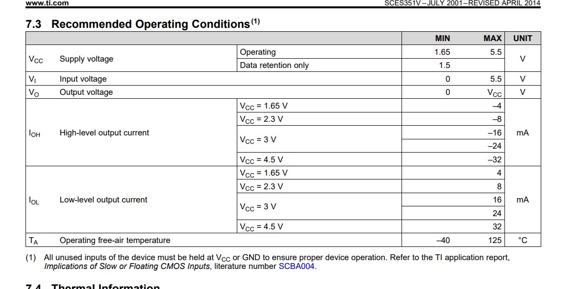
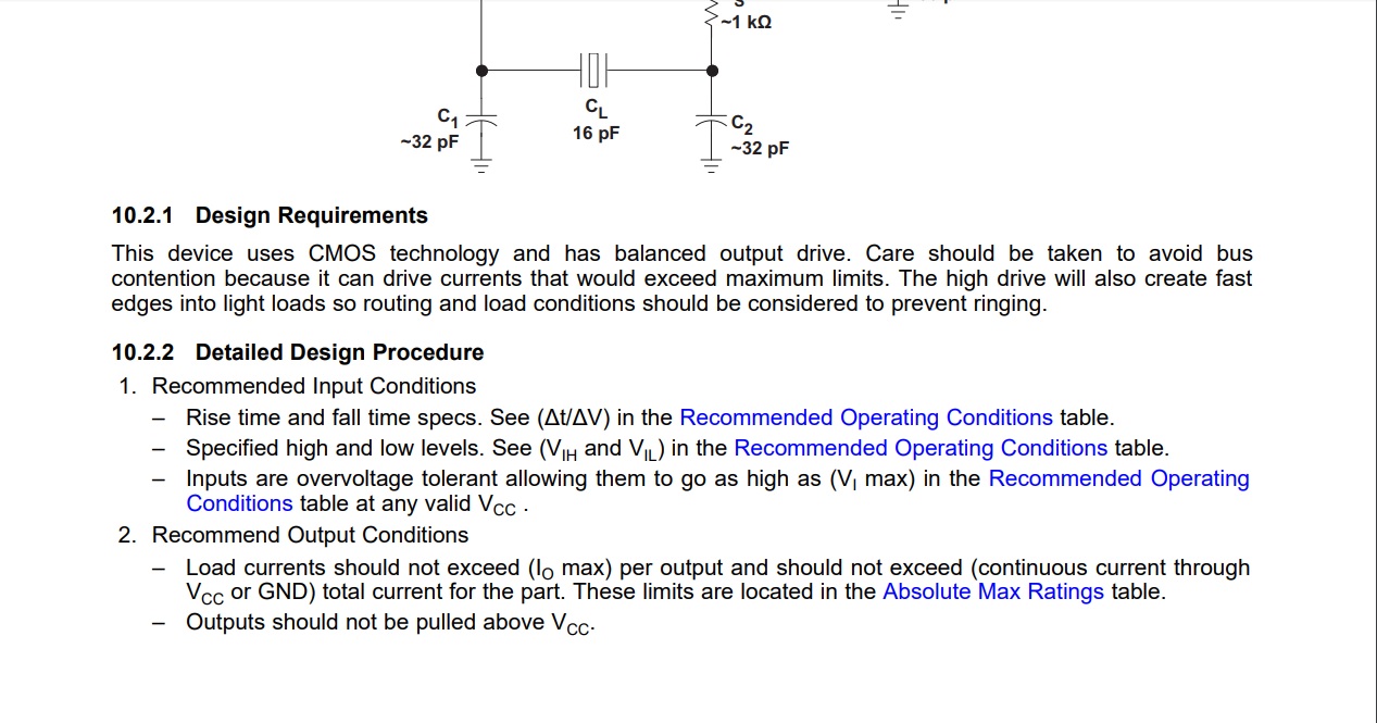
I'm planning on using this part in a design to buffer a SPI link from an FPGA to a cable.  In reading the data sheet I've gotten a little confused.  In the attached screenshot 50.jpg the data sheet says (section 10.2.2) that rise and fall times can be found in the recommended operating conditions table.  I don't see this information there.  Attached screenshot 51.jpg shows the table.

1. Where is this information?

2. How do you estimate rise and fall times of this part?

51
50
  • Hello,

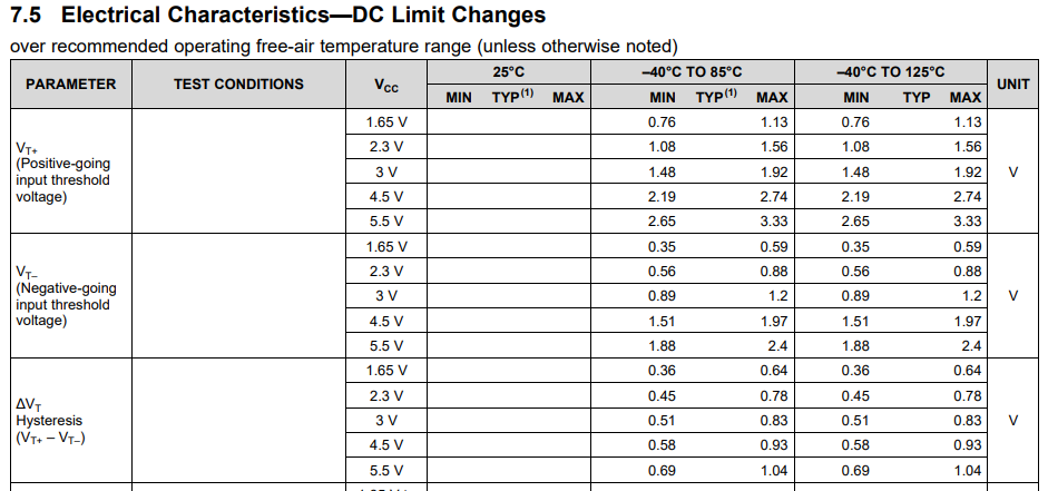
    Sorry for the confusion. I will mark this error for the next datasheet update.  Since this is a Schmitt-Trigger device, the electrical characteristics section lists the positive and negative thresholds. What this means is that this device allows slow inputs and for this reason there is no specified minimum rise and fall time listed.

    Typically there would be a input rise and fall time minimum listed for non schmitt-trigger devices. The input signal should be faster than this input rise and fall time otherwise the output would switch multiple times at the threshold and there would be large current draw. For this device, since there are separate thresholds for positive going input and negative going input, a signal at either threshold would not cause continuous switching at the output.

    Thanks!

    - Karan