Because of the holidays, TI E2E™ design support forum responses will be delayed from Dec. 25 through Jan. 2. Thank you for your patience.

This thread has been locked.

If you have a related question, please click the "Ask a related question" button in the top right corner. The newly created question will be automatically linked to this question.

SN74LV4046A: FSK Modulation / Demodulation Troubles

Part Number: SN74LV4046A
Other Parts Discussed in Thread: CD74HC4046A, SN74LVC1G17

I'm trying to do binary FSK modulation / demodulation using two SN74LV4046A, one to modulate and one to demodulate.

I built a test circuit based on the example in SLAA618 (Implementation of FSK Modulation and Demodulation using CD74HC4046A).

I've also pored over SCHA003B (CMOS Phase-Locked-Loop Applications Using the CD54/74HC/HCT4046A and CD54/74HC/HCT7046A).

VCC = 5V

On both modulator and demodulator, I am using:
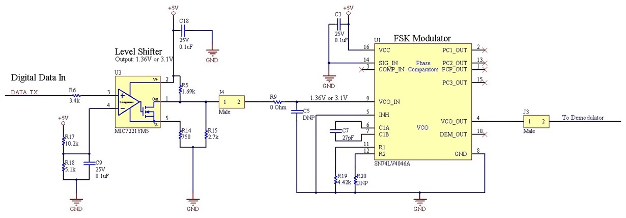
R1 = 4.42kOhm
R2 = open
C1 = 27pF

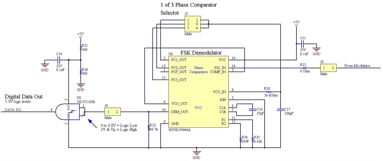
On demodulator, the low pass filter is connected as shown in figure 4 of above application note, with:
R3 = 36kOhm
C2 = 100pF

Input to the modulator is:
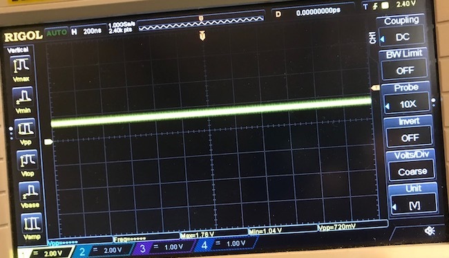
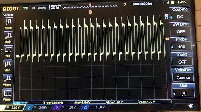
1.36V to represent binary 0 -> produces 10MHz at modulator VCO output
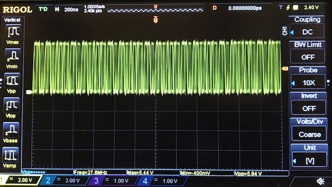
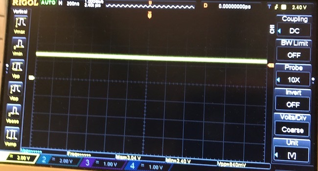
3.1V to represent binary 1 -> produces 20MHz at modulator VCO output


I am having trouble at the demodulator. I was hoping to recover approximately the same voltages as input to the modulator (or at least have good voltage separation), then use a Schmitt trigger logic gate to bring that output back to normal TTL levels.

I alternately tried using Phase Comparator 1, and Phase Comparator 2.


When using Phase Comparator 1:
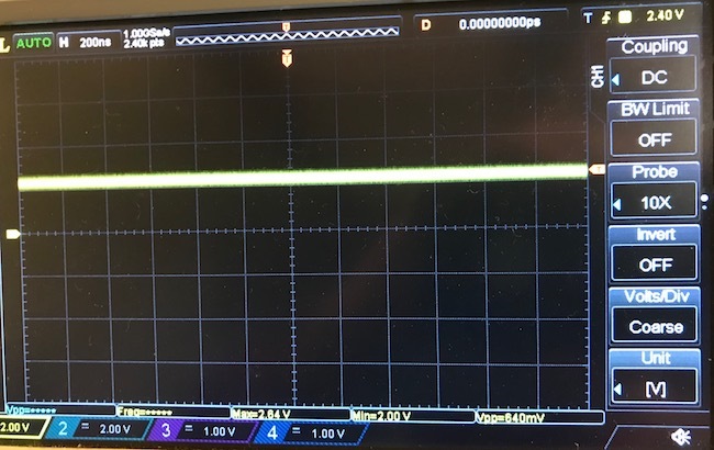
* When input to modulator is 1.36V producing 10MHz, output voltage at DEMout is about 2.75V.
* When input to modulator is 3.1V producing 20MHz, output voltage at DEMout about 2.28V.

Therefore, there is not enough voltage separation, so the Schmitt trigger logic gate does not distinguish between the two states (its output is always high).


When using Phase Comparator 2:
* When input to modulator is 1.36V producing 10MHz, output voltage at DEMout seems to oscillate at high frequency (too high for my scope) between 880mV and 2V.
* When input to modulator is 3.1V producing 20MHz, output voltage at DEMout oscillates similarly between 2.2V and 4V.

This is producing totally meaningless output.


Suggestions?

Scope images:

All of the below are using Phase Comparator 1:

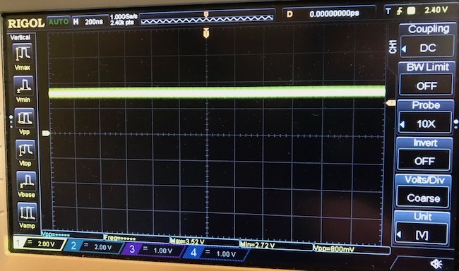
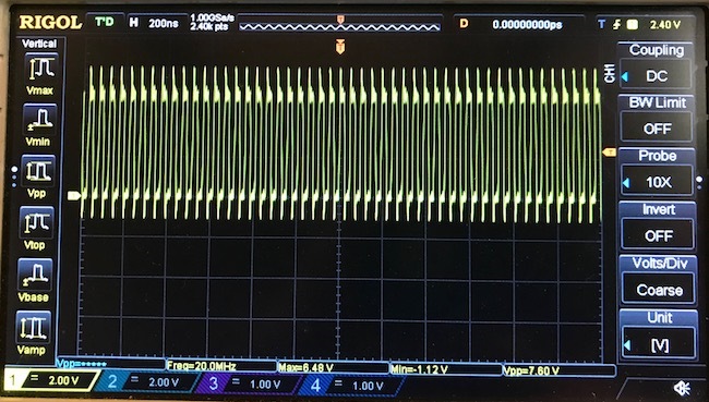
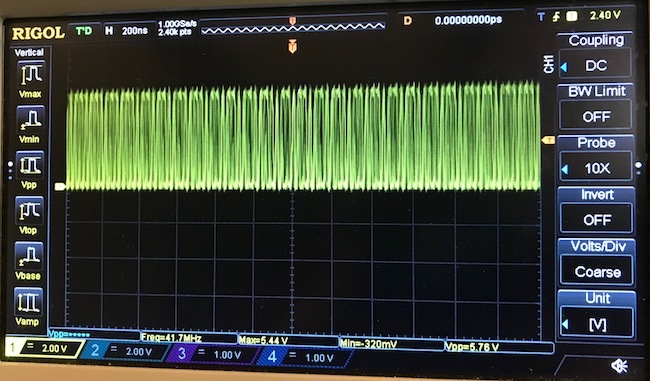
When input to modulator is 1.36V representing "binary 0":

Input to modulator VCO, 1.36V:

Modulated signal, 10MHz (9.8 MHz in this photo):

Output of Phase Comparator 1:

Output at DEMout:

When input to modulator is 3.1V representing "binary 1":

Input to modulator VCO, 3.1V:

Modulated waveform, 20 MHz:

Output of Phase Comparator 1:

Output at DEMout:

  • Hello,
    Can you provide a schematic of your circuit and an image of your test setup?
  • Thank you for your reply...

    Modulator:

    Demodulator:

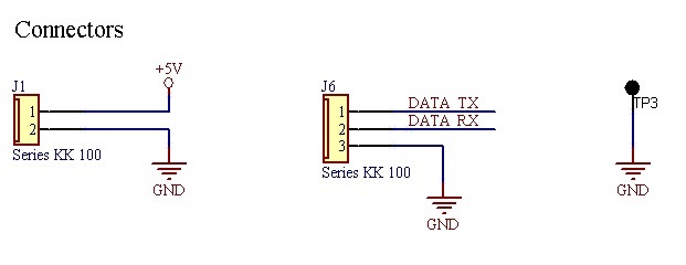
    Connectors:

  • Regarding DATA_TX and DATA_RX, the idea is to (eventually) connect those to a UART operating at 115200 BAUD -- but right now DATA_TX is connected to a potentiometer allowing to input any DC voltage from 0 to 5V to demonstrate that the level shifter is working correctly. So we are not altering the input signal at high speed at this time.

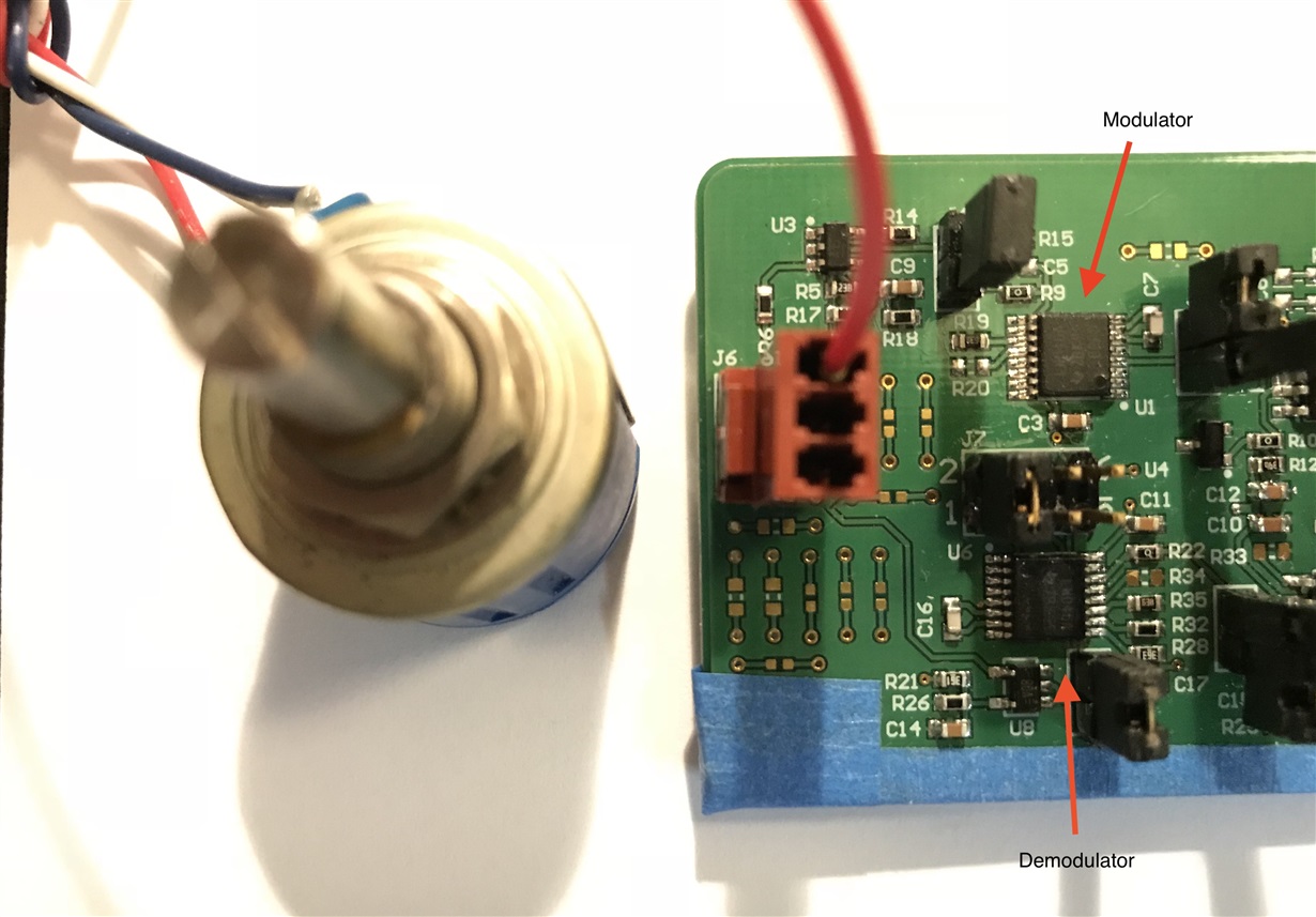
    The circuit board includes other hardware but it is not being used at this time. The jumper blocks at J3 and J8 are removed, disconnecting other hardware from the circuit, and there is a jumper wire installed from J3-1 to J8-1, which connects the modulator VCO_OUT directly to the demodulator SIG_IN.

    Circuit board:

  • Thanks for the added information.

    Can you add a low pass filter with R9/C5 to clean up the input signal a bit? I can't tell for sure, but it looks like there's about a volt of noise on that signal and it might be causing you some problems.

    There's a lot of overshoot/undershoot on your output. Is there a chance you can add a series resistance (~25 ohms) with the modulator output?

    I also noticed that you have the LVC1G08 being used as a Schmitt-trigger buffer. Just FYI, that part doesn't have Schmitt-trigger inputs. I would recommend swapping to the SN74LVC1G17 (Schmitt-trigger buffer).
  • Thanks again for your reply.

    That input signal noise concerned me as well. It is coming from a simple potentiometer and measured very cleanly without the PCB. Once the PCB is connected and powered, the noise appeared. This continued even after I played with some LPF values to smooth that huge overshoot/undershoot we saw.

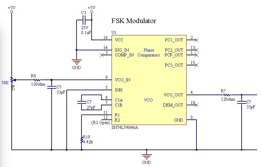
    It occurred to me that other parts in the circuit may be injecting noise into the ground, so I assembled a portion of a second PCB with only the modulator and its passives, no other ICs. I populated R9/C5 at the VCO input with a 120ohm 33pF LPF and I added the same values at the modulator output. The modulator output is now rounded off quite a bit.

    I've also gotten much better oscilloscope images by saving them from the scope rather than snapping photos with my phone!

    The noise at the potentiometer input is much reduced but it is still as high as 320mV p-p.

    I'll attach the new modulator images for reference and then I'll populate the demodulator section and we'll see what happens.

    In the meantime I appreciate any thoughts or suggestions.

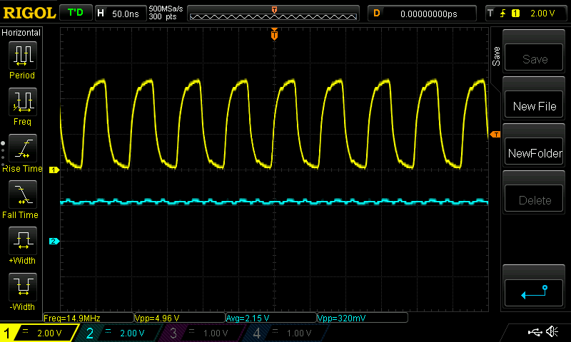
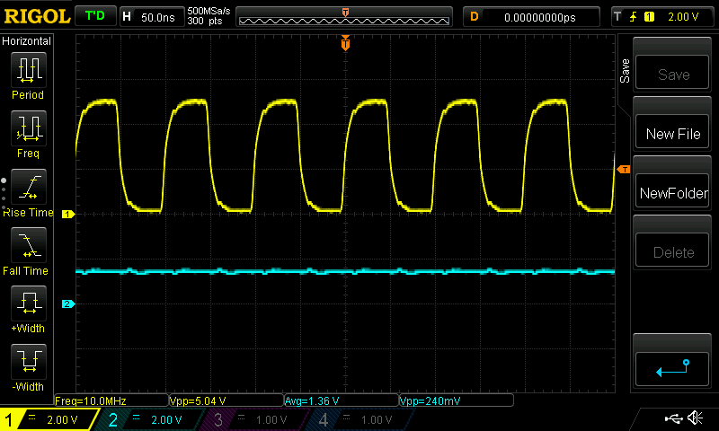
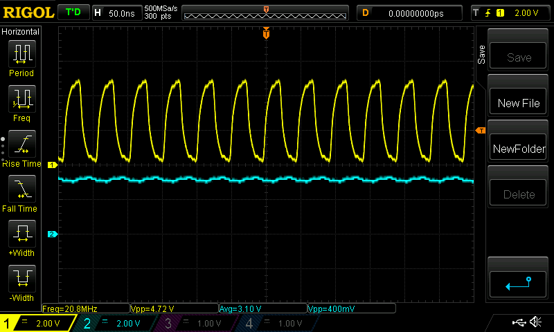
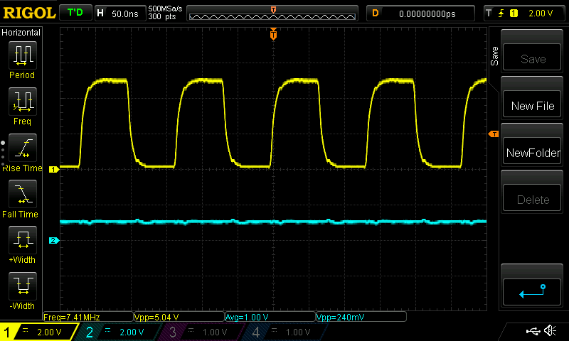
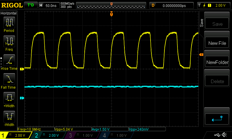
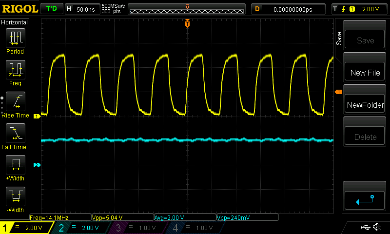
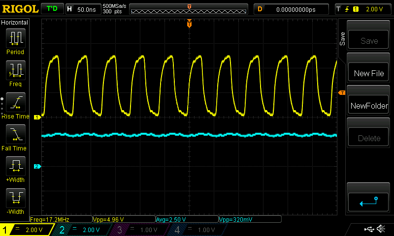
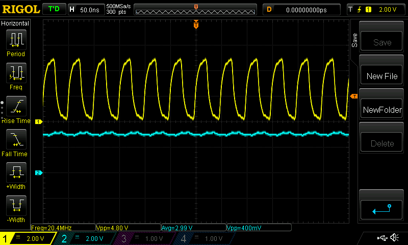
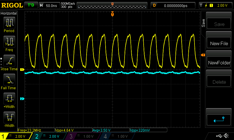
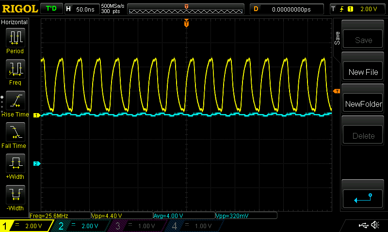
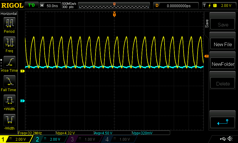
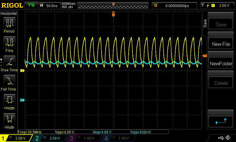
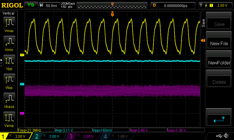
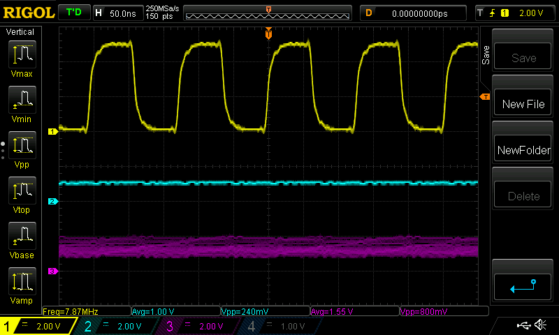
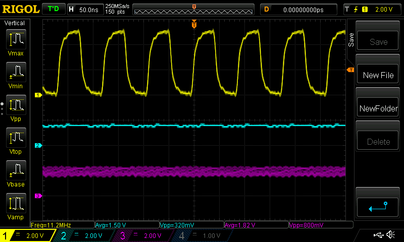
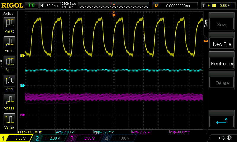
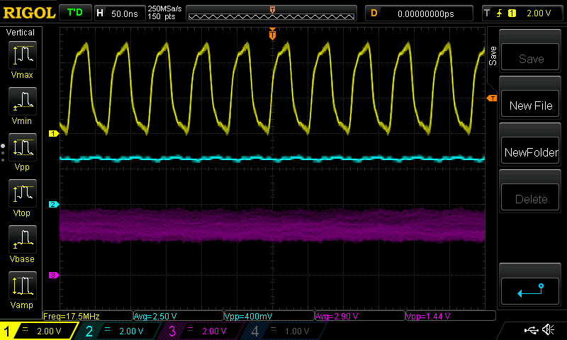
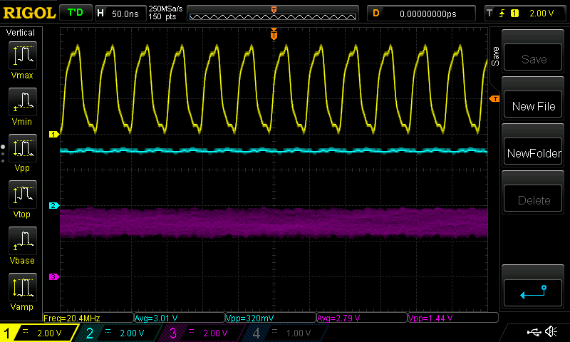
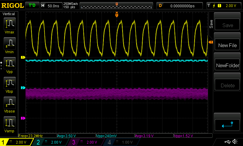
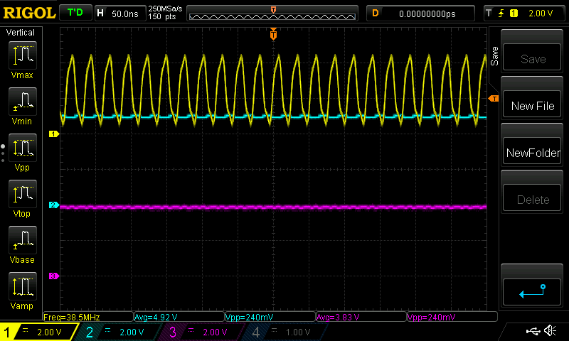
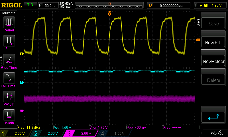
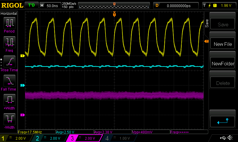
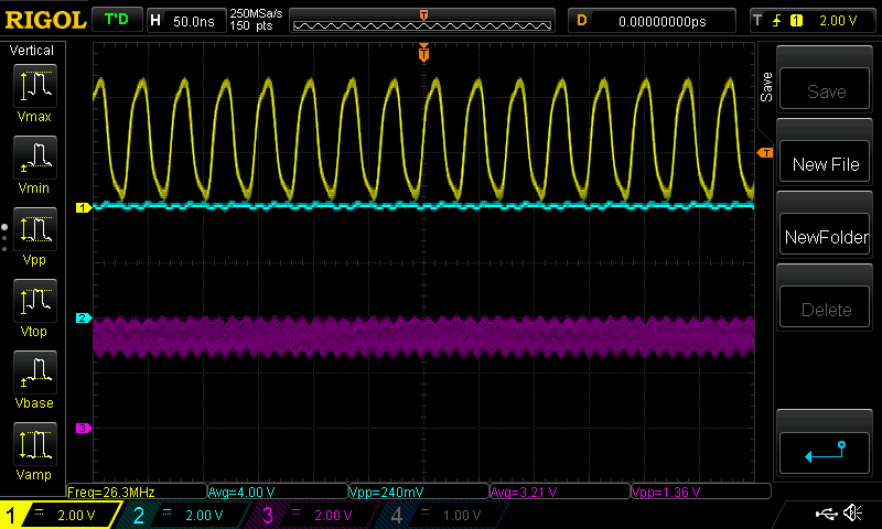
    Oscilloscope images below show:
    * Channel 1 = modulator output (yellow)
    * Channel 2 = VCOin from potentiometer (blue)

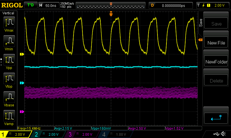
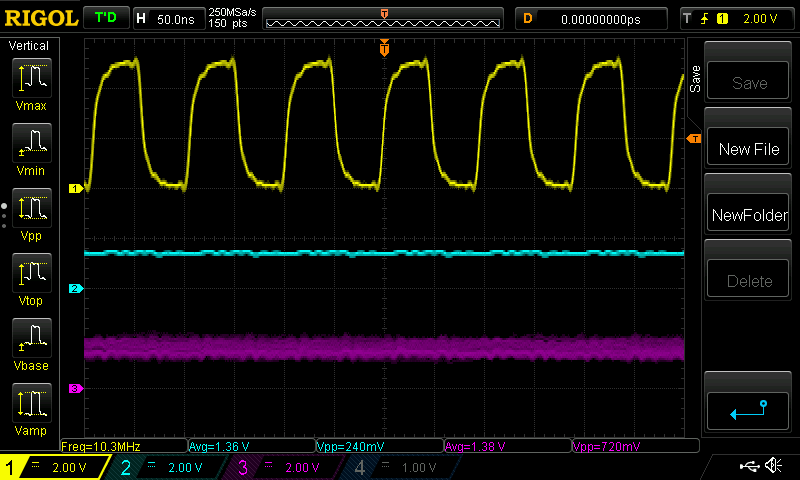
    At the bottom of each screen capture, you can see the readouts of modulator frequency (Freq, yellow), modulator output peak/peak voltage (Vpp, yellow), VCOin voltage (Avg, blue), and noise on VCOin (Vpp, blue).

    Screen captures are shown in this order:

    The values we (currently) intend to use in the real application:

    • * Center frequency at 2.15V VCOin is about 15 MHz.
    • * VCOin of 1.36V (meant to represent "binary 0") gives 10 MHz.
    • * VCOin of 3.1V (meant to represent "binary 1") gives 20 MHz.

    Followed by other values of VCOin / frequency out for reference:

    • * 1V = 7.41 MHz
    • * 1.5V = 10.9 MHz
    • * 2V = 14.1 MHz
    • * 2.5V = 17.2 MHz
    • * 3V = 20.4 MHz
    • * 3.5V = 23.2 MHz
    • * 4V = 25.6 MHz
    • * 4.5V = 32.2 MHz
    • * 5V = 38.5 MHz

    (These frequencies are different than what I calculated using SCHA003B but I recognize that that application report discusses the older CD54/74HC/HCT4046A.)

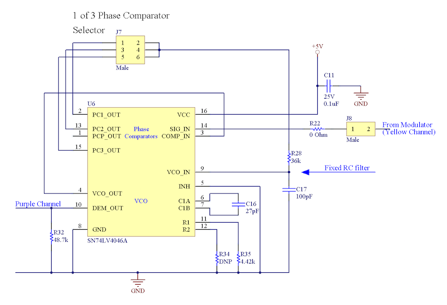
  • Schematic of the reduced circuit I have now -- see oscilloscope captures and explanation in previous post:
    I'm going to populate the demodulator 4046A and its passives... be back soon

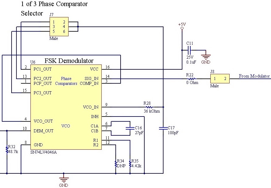
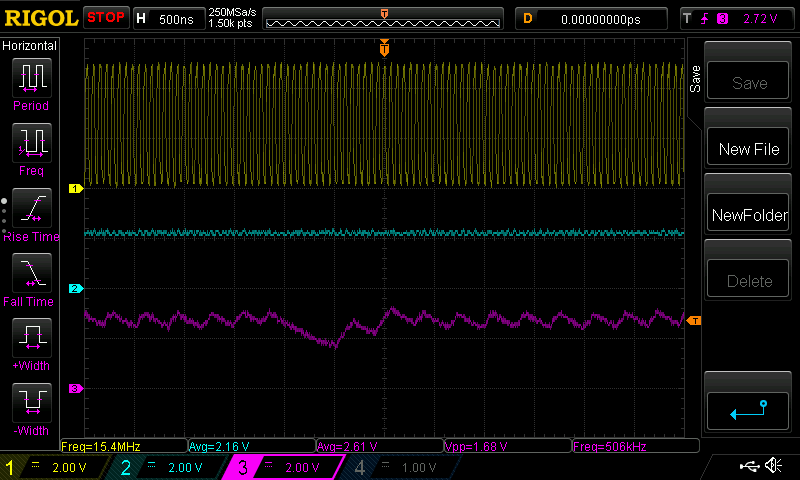
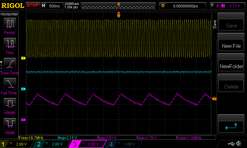
  • I assembled a PCB that has only the modulator and demodulator and their passives (no other ICs) to eliminate anything that might have introduced noises etc. The previous two posts document assembly and measurements of the modulator. Now I added the demodulator as shown in the following schematic:
    Results are very similar to before: the DEMout output is unusable for recovering the input signal to the modulator. There must be some mistake in the design.

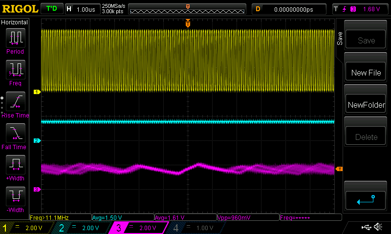
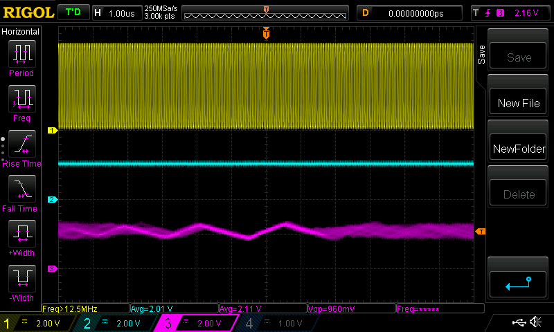
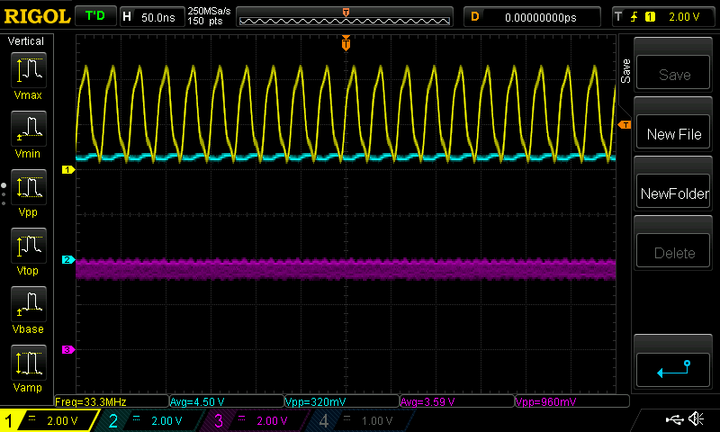
    Oscilloscope Captures

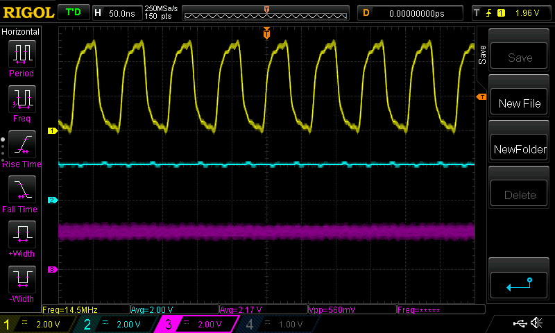
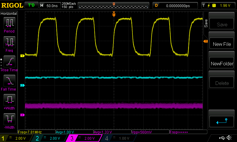
    • CH1 (Yellow) = Modulator VCO_OUT
    • CH2 (Blue) = Modulator VCO_IN
    • CH3 (Purple) = Demodulator DEM_OUT

    Once again, I am showing the captures in the following order:

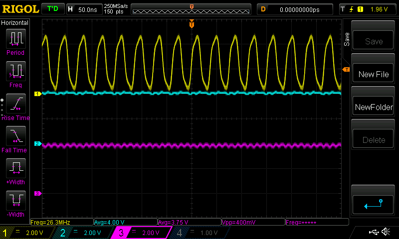
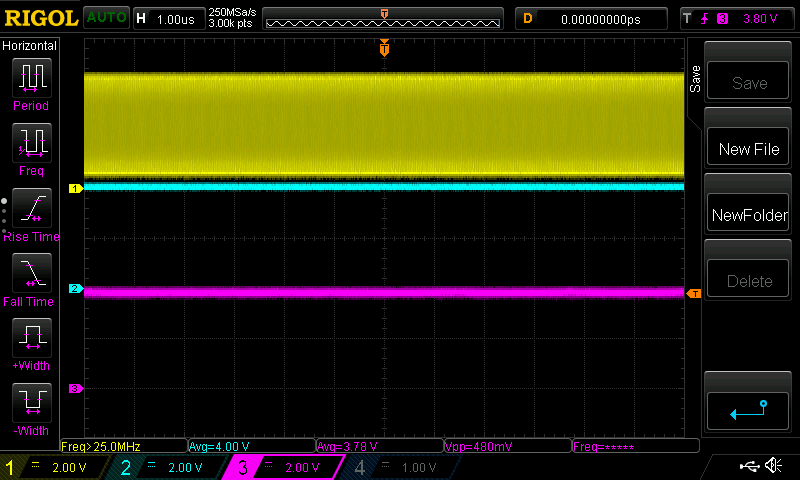
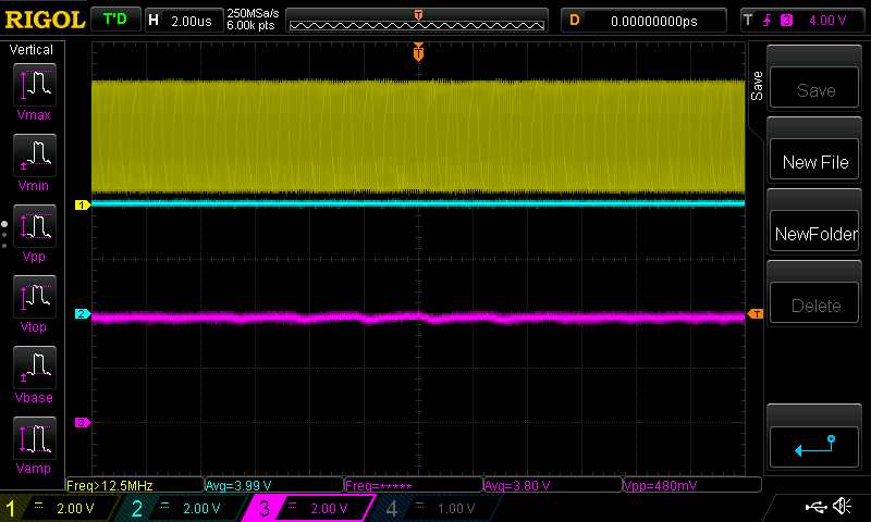
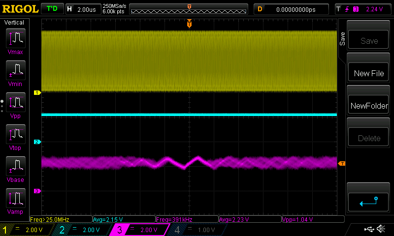
    • VCO_IN at Modulator is 2.15V (center frequency)
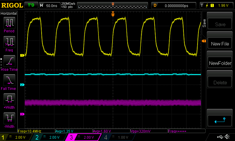
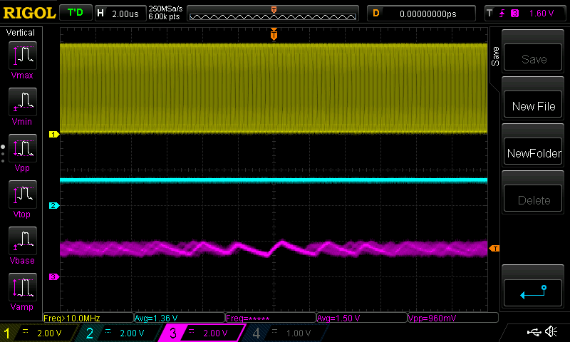
    • VCO_IN at Modulator is 1.36V (represent binary 0 at modulator)
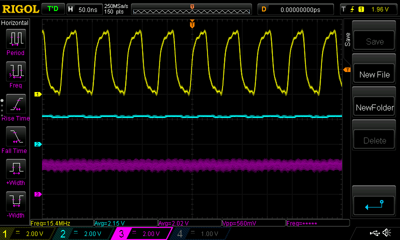
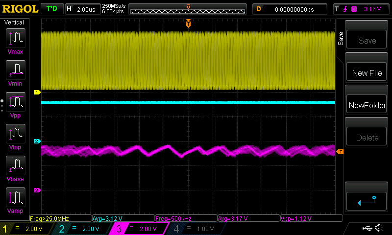
    • VCO_IN at Modulator is 3.1V (represent binary 1 at modulator)
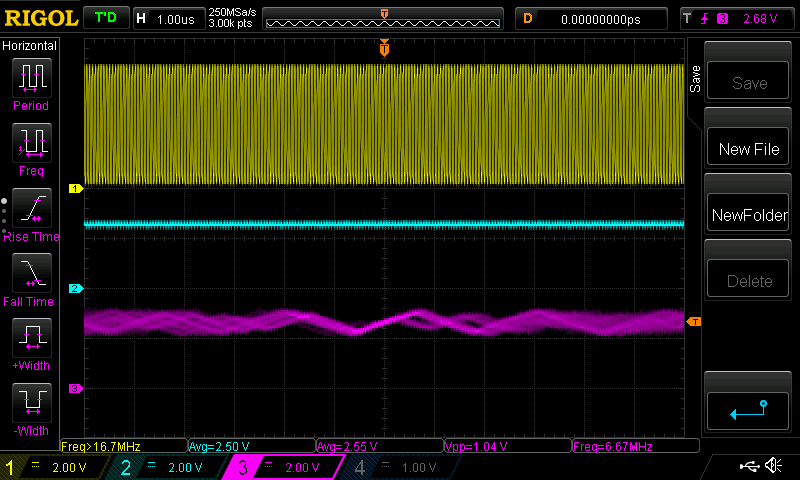
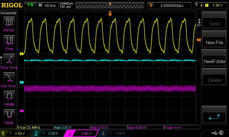
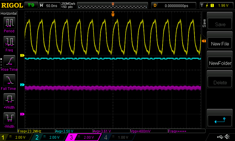
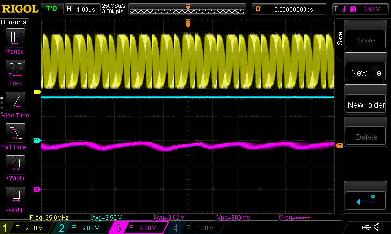
    • VCO_IN from 1V to 5V in steps of 0.5V to give an idea of the circuit's behavior.

    I am showing results for Phase Comparator 1 followed by Phase Comparator 2.

    Measurements at the bottom of each oscilloscope capture show:

    • Freq (Yellow) = Frequency of Modulator VCO_OUT
    • Avg (Blue) = Average voltage of potentiometer input to Modulator VCO_IN
    • Vpp (Blue) = Volt peak-to-peak of potentiometer input to Modulator VCO_IN
    • Avg (Purple) = Average voltage of Demodulator DEM_OUT
    • Vpp (Purple) = Volt peak-to-peak of Demodulator DEM_OUT

    Please let me know if you need any other measurements from the circuit.

    Thanks for helping.

    Using Phase Comparator 1 at Demodulator:

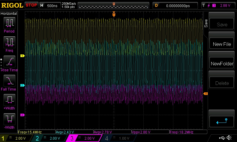
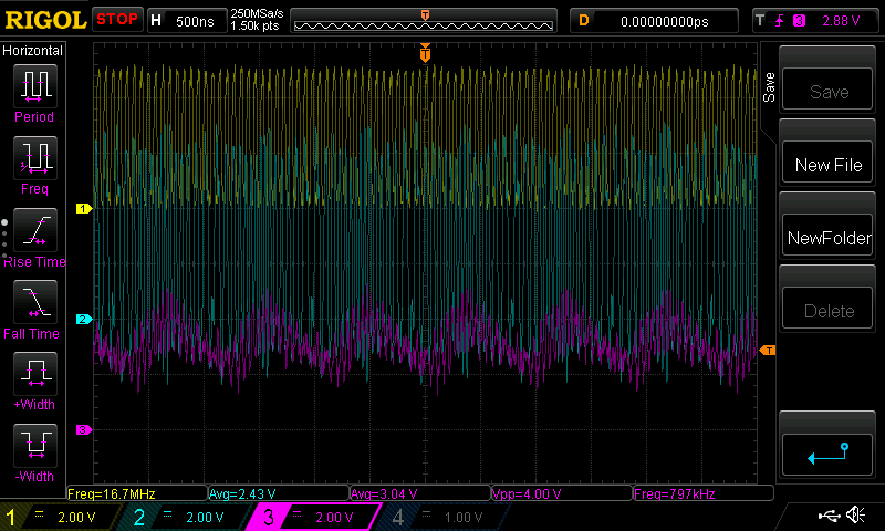
    Using Phase Comparator 2 at Demodulator:

  • I noticed that the RC filter on the output of the phase comparator is reverse:

    The input at pin 9 likely has 5 to 10pF of input capacitance, so you're still getting some filtering, but the corner frequency is probably a decade higher than you would like.

    If it's possible, can you grab a scope shot of the DEM_OUT when it's really ugly and trigger off that? I'd like to see what frequency it's oscillating at and how that relates to the VCO output.  They seem to be unrelated.

    Also, can you try reducing the size of R32?  I'm wondering if adding some load to the unity gain amplifier between VCO_IN and DEM_OUT will kill that oscillation you're seeing.

  • Thanks again for your input.

    You are absolutely right about the RC filter being backwards. I have been looking at this circuit for days and never saw it! Thank you for seeing it!

    Obviously I will need to fix that. It looks like that will require cutting some delicate work, so before I do that, I will grab the scope shot for you of DEM_OUT as the circuit stands now. Then I will go perform some surgery.

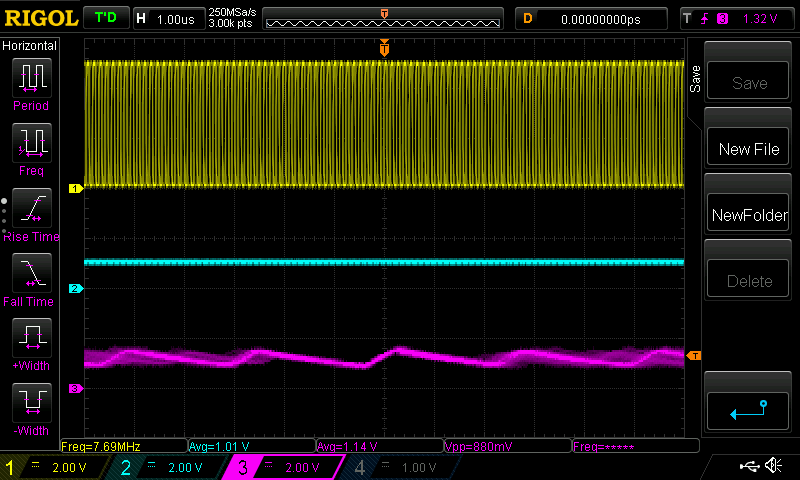
    There are two scope shots here, showing what happens with Phase Comparator 1, then Phase Comparator 2.

    • Channel 1 (Yellow) - Modulator VCO_OUT
    • Channel 2 (Blue) - Modulator VCO_IN
    • Channel 3 (Purple) - Demodulator DEM_OUT

    I'm triggering off DEM_OUT. I changed the timebase to 500ns so we can see that signal a bit better.

    Again, these captures are before making any changes to the circuit.

    With Phase Comparator 1:

    With Phase Comparator 2:

    DEM_OUT here is usually 1.1 MHz but occasionally goes to about 1.3 MHz for a brief moment, then returns to 1.1 MHz.

    I also tried to use channel 2 (blue) to capture the VCO_OUT of the demodulator instead of VCO_IN of modulator, but that just creates a mess, I'm guessing because of added capacitance from my scope probe. This is with phase comparator 1:

    And with phase comparator 2:

  • It looks like the unity gain buffer is becoming unstable.

    This is usually caused by an excessive capacitive load, but I'm wondering if the slow input to the LVC1G08 is having an effect as well due to internal oscillations and transfer through the supply or ground.

    Can you try measuring DEM_OUT with the jumper J9 removed? Or even better, with U8 removed? Preferably with a low capacitance probe.
  • Emrys Maier said:

    It looks like the unity gain buffer is becoming unstable.

    Which of the scope captures in my previous post show that the unity gain buffer is becoming unstable? Is it the first two or the last two?

    The last two scope captures showed the mess that resulted when I attempted to measure VCO_OUT of the demodulator. I think that is the result of added capacitance of my scope probe.

    Emrys Maier said:

    This is usually caused by an excessive capacitive load, but I'm wondering if the slow input to the LVC1G08 is having an effect as well due to internal oscillations and transfer through the supply or ground.

    All of the above scope captures are from the second board I constructed, which has only two SN74LV4046A: one for the modulator, one for the demodulator, and their passives. There are no other ICs on this board, including no LVC1G08.

    I did that because on the first board, it looked like there was a lot of noise on the ground. I wanted to eliminate the possibility of other ICs interfering with the modulator / demodulator pair -- until after I get them working correctly.


    Emrys Maier said:
    Can you try measuring DEM_OUT with the jumper J9 removed? Or even better, with U8 removed? Preferably with a low capacitance probe.

    Tomorrow morning I will be at the lab. I need to fix the incorrect low pass filter, which you pointed out is reversed. I made the above scope captures first so that we'd have a baseline for comparison.

    Also I haven't (yet) tried your suggestion to put a stronger load resistor on DEM_OUT. I think I should fix the low pass filter first, then get some scope captures, and then if still necessary experiment with the DEM_OUT load resistor.

    I'll try to minimize scope probe capacitance.

    Thanks again for your continuing help.

  • The oscillation appears in all of the DEM_OUT scope shots to one degree or another. The output of a unity gain buffer should be the same voltage as that put into it, and we're seeing oscillation instead.

    I spoke with a friend here who is an expert on op amps, and his recommendation was to isolate any capacitive load from the opamp's output with a 100 ohm resistor (series - between the pin and the load resistor node). He also suggested trying an increase in the load resistance (the opposite of my suggestion).

    Another suggestion he had was to isolate the buffer and force a square wave input to it (~1V amplitude, DC offset of 1/2*Vcc). Any ringing on the output waveform could show us how unstable the internal circuit is. This would allow for trying different probe and output load configurations to improve stability.
  • Thank you very much for your continuing help.

    Now we're making some progress!

    I've done a bit of surgery on the board and fixed the reversed RC filter on the output of the demodulator phase comparator.

    I have not made any further changes to the modulator.

    I have not (yet) taken your friend's advice, but I will do that after I show how different everything is with a corrected filter.

    Schematics of what I have now:

    Modulator, unchanged since we added the RC filter on VCO_OUT:

    Demodulator, with the RC filter corrected:

    I've taken quite a few scope captures.

    All of the following scope captures use:

    Channel 1 (Yellow) is modulator VCO_OUT.

    Channel 2 (Blue) is modulator VCO_IN, measured at the pot. (It would probably look nicer if measured at the VCO_IN pin, but I didn't have a convenient way to measure it there.)

    Channel 3 (Purple) is demodulator DEM_OUT.

    Phase Comparator 1 (PC1)

    PC1 doesn't seem to do anything useful right now. Regardless of modulator VCO_IN, demodulator DEM_OUT remains stuck at 2.57V, with only a slight change when modulator VCO_IN is 2.6V. Here's an example, when VCO_IN is 2V:

    I don't know if it makes sense to diagnose PC1 further right now, because PC2 seems to be doing better...

    Phase Comparator 2 (PC2)


    PC2, on the other hand, seems to have improved by fixing the RC filter. I did not yet take the additional steps your friend advised. I will do that next.

    I took scope captures at these modulator VCO_IN values:

    • From 1V to 4V in 0.5V steps
    • 1.36V (my binary 0)
    • 2.15V (center frequency)
    • 3.1V (my binary 1)

    What we see in these screenshots is that when modulator's VCO_IN is in the range 1V through about 3.7V, demodulator's DEM_OUT follows it (with a little bit of offset, and putting other signal quality issues aside for a moment). That's a big improvement.

    1V VCO_IN

    I show two scope captures each:

    • Triggered on modulator VCO_OUT (timebase 50ns)
    • Triggered on demodulator DEM_OUT (timebase 1us)

    I hope that is not confusing!


    1.5V VCO_IN:

    2V VCO_IN:

    2.5V VCO_IN:

    3V VCO_IN:

    3.5V VCO_IN:

    4V VCO_IN (DEM_OUT doesn't continue increasing at this point -- frequency too fast to lock?):

    For the following I forgot to get a 2nd screenshot triggered off of DEM_OUT, but it's very similar to those above.

    1.36V (represent binary 0 at modulator):

    2.15V (center frequency):


    3.1V (represent binary 1 at modulator):

    Next up, I am going to try your friend's advice of adding a 100 ohm series resistor between DEM_OUT and the load resistor, and increasing the load resistance value. Be back soon...

  • Thanks for the update.  I've ordered some samples so I can take a look at the DEM_OUT pin myself. Hopefully I can reproduce your results here in the lab.

  • I doubled the DEM_OUT resistor to GND from 48.7k to 100k.

    I also added a 100 ohm resistor to the board and intended for it to be a series resistor on DEM_OUT before the 100k to GND, but when I placed the correction wires, I got confused and bypassed it. So we have the 100k to GND but not the 100 ohm yet. I'll fix that in the morning.

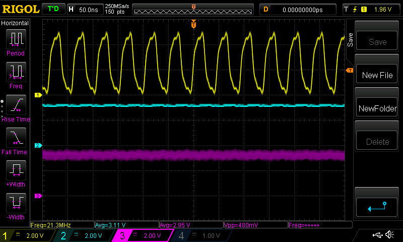
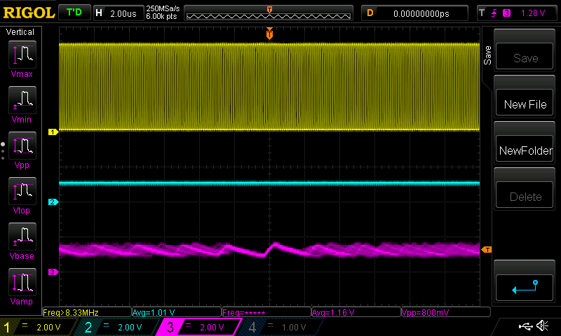
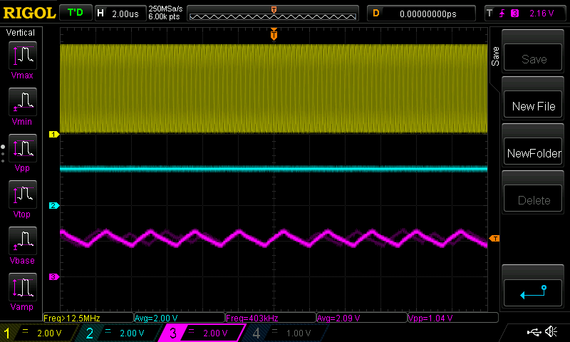
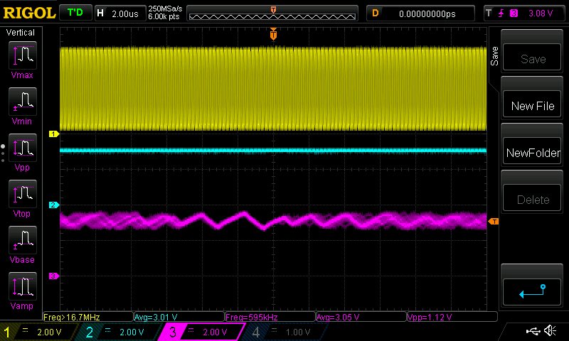
    Meanwhile here are some scope captures of DEM_OUT at the demodulator for various values of VCO_IN at the modulator:

    VCO_IN = 1V, DEM_OUT is average 1.16V with 800mv p-p:

    VCO_IN = 2V, DEM_OUT average 2.09V with 1.V p-p:

    VCO_IN = 3V, DEM_OUT = 3.05V with 1.12v p-p:


    At 4V VCO_IN we're out of range on DEM_OUT as we learned in previous posts...

    The important VCO_IN values:

    1.36V to represent binary 0 at modulator gives average 1.5V with almost 1V p-p at demodulator:

    2.15V to generate center frequency at modulator:

    And 3.1 V to represent binary 1 at modulator gives about 3.17v with 1.12v p-p at demodulator:

  • I have my samples now - next week when I'm in the office I will get into the lab and see if I can replicate the issues you're having.

    I've never run into the issue you're having here -- hopefully we can find a fix, but if it turns out to be something internal to the IC that we can't change, you could try swapping to the SN74HC4046. There are a few devices with the same pinout/function that are (basically) interchangable. The only other option I can think of is to use an external opamp to buffer the signal. I'd consider that a last resort since that would require you adding another socket to the board.
  • I appreciate your help and I'll be eagerly waiting to hear of any discoveries you make. Meanwhile I'll keep you posted if I discover anything new on my end.
  • I just wanted to make a quick post to let you know I haven't forgotten about this.

    With the recent holiday, I've been very busy and haven't been able to get into the lab. I still plan to test this buffer to see if I can replicate the issue you are seeing.
  • Thank you -- both for not forgetting and for keeping me posted. I appreciate your help very much.
  • Have you had a chance to experiment with the SN74LV4046A samples?
  • No - I'm afraid that I have not had time to get into the lab yet. I'm currently planning to spend all day tomorrow in there catching up on all the tests I need to do, including this one.

    I just completed a final exam for my analog IC deesign course (hooray!), which I had taken a day off work to study for. Working full time and working towards a master's degree is rough!
  • For an update: I was able to get my bench setup about 1/2 completed today. It was quite an exciting day (unfortunately) and a bunch of issues that required my immediate attention kept popping up.

    I'm going to be back in the lab tomorrow to get some data.
  • To give you a brief update:

    I was able to test the device on the bench today. I found that the buffer used only has a valid input range from 0.7V to ~3.6V -- beyond 3.6V input I see a ton of noise/oscillation on the output. It looks like you are using it in the right range from the scope shots, so I doubt that's the problem.

    My initial tests were all done with the VCO disabled (no RC components attached), so my next step will be to get it running at a similar frequency to yours and see if I can reproduce the noise you're seeing.
  • Thank you for the update. I am glad that we are operating within the valid input range on the buffer.

    Looking forward to hearing if your setup, with VCO enabled at similar frequencies to ours, exhibits the same issues we're seeing. Thanks again.
  • Hey,
    I was able to get the device operating in a very similar condition to yours (10 MHz VCO frequency, slightly different RC values), but I wasn't able to get the same type of instability for the DEM_OUT buffer.

    I've tried adjusting the output loading with different capacitances and resistances (no load to ~100pF, open to 100kohm).

    I'm not sure what else I can try. Sorry I'm not more help!
  • In a way this is actually encouraging because it means we should be able to get good output.

    Were you able to get any scope captures so we would know what we could hope to shoot for?
  • Unfortunately that day my USB drive wandered off so my only scope shots were with my phone.  Sorry for the poor quality:

    The yellow signal (ch 1) is the trigger and the output at VCOOUT.

    The green signal is the input (DC source) to VCOIN.

    The blue signal is the output at DEMOUT.

    The noise was pretty consistent regardless of my input voltage until I went outside the buffer's common-mode range:

    In this one green is the DC source input, yellow is the buffered output.

  • Apologies for my delayed response. Thank you for all your help on this. I think we are very close to having it work properly. My colleague believes that a portion of the noise we're experiencing at this point is due to correction wires (a few of which are somewhat lengthy) and some other funny things I had to do on the circuit board to add passives, correct the RC filter, etc. So we're probably going to build a new PCB incorporating all the fixes and lessons we learned here (and with better routing!) and test again in the near future. Thanks again for your help.
  • Happy New Year!

    Thanks for getting back to me, and for marking this as resolved.

    I am always happy to help. Come back any time!

  • Emrys Maier said:

    Happy New Year!

    Thanks for getting back to me, and for marking this as resolved.

    I am always happy to help. Come back any time!

    I will most likely be back with (lots) more questions!!!!

    Thanks again for all your help. Happy New Year!