This thread has been locked.

If you have a related question, please click the "Ask a related question" button in the top right corner. The newly created question will be automatically linked to this question.

TXS0102: Bidirectional level shifter that can handle VCCA=3.3V to VCCB=2.4V, and 5V

Part Number: TXS0102
Other Parts Discussed in Thread: USB2ANY, TXB0302, LSF0102

Hi,

I am trying to interface 3.3V USB2ANY I2C with a voltage rail that starts @ 2.4V, then ramps up to 5V. I was initially using the TXS0102, tying VCCA=3.3V USB2ANY side and tying VCCB to the other side (2.4V -> 5V). The issue that we overlooked was that the TXS0102 only works with VCCB>VCCA, which is not the case when VCCB=2.4V (note VCCA=3.3V always since it is coming from the USB2ANY I2C). 

I saw the previous question suggesting the TXB0302 may be a good option. The issue with this device is its max voltage on either side is 3.6V, which won’t work for my application which needs 5V on one side. Is there one similar with a max voltage  that can handle my application requirement of 5V?

Basically, I am looking for a level translator to be used for I2C communication – so it needs to be bidirectional (no direction pin). It needs to interface the 3.3V USB2ANY with a voltage rail that varies from 2.4V to 5V, so the VCCA can be greater or less than VCCB. Is there a level shifter that does this? What are my options?

Thanks,

Luke

  • Hi Luke,

    I would recommend the LSF0102 configured in the "single supply" operation mode, so all you need is one stable supply.  It's a little complex if you've never used it before, but there's a great video series on designing with the LSF translators located here:  

  • Hello,

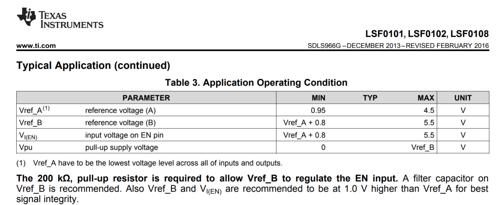
    I would like to reiterate, I need to translate SDA/SCL I2C logic from one supply of 3.3V to another supply that varies from 2.4V to 5V.  Reading through the datasheet of the LSF0102, it looks like VREF_A must always be lower than VREF_B: see picture below. This is not acceptable for my application. Is there a way to get around this?

    Thank you,

    Luke

  •  Hi,

    Sorry I did not watch the video. It looks like the VREF_A side is being generated using a resistor divider set to the lowest voltage in the system (2.4V). What exactly is going on under the hood? Meaning what do the circuits look like on the chip that are driving the A1 and A2, and what are their power rails?

    Thanks

    Luke

  • In other words, can we do the same thing (add the R1 and R2 to VREF_A so VREFA=2.4V) with the original TXS0102? If not, why can't we do it with the TXS0102 and why can we do this with the LSF0102?

    Thanks,
    Luke
  • Hey Luke,
    The other videos in the series go through every single transistor in the device. I couldn't explain it any better or faster here.
  • Hey Luke,
    Sorry for the double reply -- I should have just put this in my first response.

    You asked why we can't do this with TXS0102. It's because TXS0102 is a __much__ more complex device than LSF0102. The TXS0102 has over 2000 transistors in it for internal logic. The LSF0102 has 3 transistors in it. I would highly recommend watching at least the first two videos in the LSF series. They should answer all your questions.