


Hi Dear expert,
My customer uses TXB0304 on their board. Below is the schematic.
I/OVLx is input signal, coming from FPGA, for each input, there is 20K resistor to GND which is not shown below. I/OVCCx is output, going to RF device working as a control signal. Near the RF device, customer also connect a 10pF cap to GND. The output trace is 30cm long. The input trace is also very long, 15cm.

We met two problems, one we have known the root cause. The issue is there is ringing at the output signal. It is due to long PCB trace which have large reflection, I suggest customer to remove the 10uf caps to GND near the RF device, and add the serial resistor at the output, we increase the resistor to 1.5K and the ringing is off. However, it make the low to high and high to low slew rate very low.
See below pic: Before removing cap and add 1.5K resistor:

After removing the cap and add 1.5K resistor:

Can you please confirm the root cause we think is correct? Do we have ways to make the high to low and low to high slew rate higher?
Second issue we have found is that sometimes, the output will show sine wave like below:
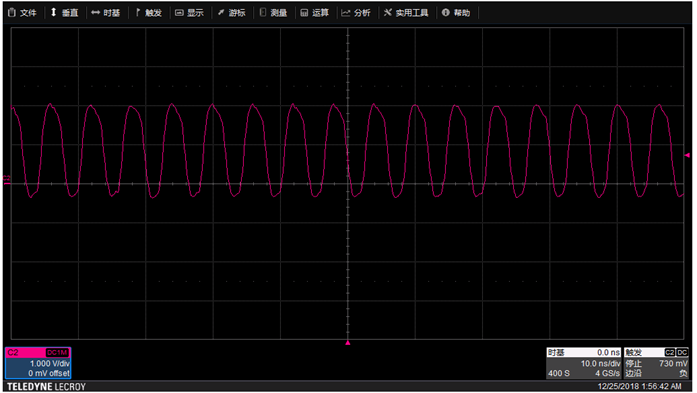
If we use probe to touch the output, the output will become correct level. but the input wave is looking like sine wave.
Do you know why output looks like sine wave?
thanks for your reply!
BR, Joyce

