This thread has been locked.

If you have a related question, please click the "Ask a related question" button in the top right corner. The newly created question will be automatically linked to this question.

SN74HC165-Q1: Inquiry about internal block

Part Number: SN74HC165-Q1

HI team.

My customer designed SN74HC165-Q1 without connecting GND.

They proceeded to mass production with a mistaken circuit.

But, It does operate actually output depending on Input.

So, customer has question how did operate without connecting GND.

They want to explicate through Internal Block or circuit.

Thank you.

  • Hi Charles,

    Surprisingly, this isn't the first time I've seen this issue.

    All the answers are in the image you have provided and the datasheet, but I will be happy to walk through it.

    First, it's important to know that this device has negative clamp diodes (just like every other CMOS logic device):

    You can see from the above table that the datasheet lists a maximum clamp diode current of 20mA for the case of VI < 0V. This indicates the existence of the diode.

    The next important thing to notice is that the CLK_INH pin is a standard CMOS input:

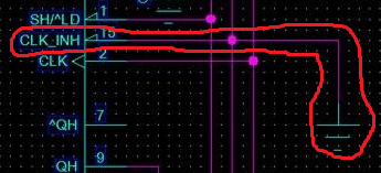
    Also, we can see from your image that the CLK_INH pin is connected directly to ground:

    Finally, we can put together this information to show what's going on:

    In the above simplified diagram, I have only shown one CMOS input (CLK_INH) represented as a CMOS inverter, and one generic output (Qx) (also represented as a CMOS inverter). This is a very typical structure for standard logic devices.

    Current would normally flow from VDD, through the internal logic, then out through the GND pin, as shown by the orange and red arrows above.  Since the ground pin is not connected, the return current cannot flow that way, so it finds a different path. The green arrows show how the return current flows through the input negative clamp diode, then into ground as usual.

    This can be problematic for several reasons.

    (1) The diode is only rated to 20mA, while the ground pin is rated to 50mA. This can affect reliability if the total sink current of the device is larger than 20mA.

    (2) Current flowing through the diode produces a voltage drop, which will shift the operating voltage of the HC165. In most logic systems this isn't a big issue, however it can cause excessive current in subsequent stages.

    (3) Since the input was not really designed to provide a low impedance path to ground (in fact, it's designed as a high-impedance input), it's likely that all negative transitions have been significantly slowed, which again likely won't cause any big issues, however many CMOS system have limitations on input transition rates.

    As a fix, I would recommend connecting the ground pin -- from your post I assume you already know this, but I have to make an official recommendation.