This thread has been locked.

If you have a related question, please click the "Ask a related question" button in the top right corner. The newly created question will be automatically linked to this question.

SN74LVT16245A: spurious ground bounce

Part Number: SN74LVT16245A
Other Parts Discussed in Thread: SN74LVT16245B,

We are using TWO number of 74LVT16245A chips to

buffer a0-15 address lines in one of the device, which is always enabled

and 

buffer a16-19, RD, WR signals + d0-7 signals from another device

This device is controlled, and the direction of d0-7 is also controlled using RD signal.

These are addressing 16 cards, having 22V10 PAL on A10-a19,  74hct245 on D0-7 and IDT7130 on a0-a9 + RD=WR

This scheme is working in system and addressing 16 cards from 2008 in the field.

When we recreated the same, [with new backplane and new PAL ATF22V10C-15PU] 

We are struggling for last 3 weeks, with spurious write taking place due to

1. ground bounce on a10-a19 which are used to generate CHIP Select signal.

The ground bounce occurs, when more number of lines change to 0. Like

address xx00 or xx80 or xxc0

or when data to be written is 00, 80, 40 RANDOMELY

We tried Termination from 220R to 10K

We tried Pull up from 2k2 to 10K

we tried pull-up 2k2+pull down 3k3

The problem remains same, it occurs once in 16000 or 40000 or 160000 writes.

How to resolve.

We checked with series resistance of 33R, or 68R or 220R, none helps

  • The schematic does not have decoupling capacitors. Please show where you've placed them on the board layout.
  •  Thanks for pointing out.

    Each of the 74LVT16245 has FOUR 100nF/50V 0805 X7R type decaps.

    We tried adding bulk capacitors along with of 47uF, 10uF, 100uF, Tantalum as well as electrolytic.

    We noticed the backplane pcb tracking, to be new and although we isolated and connected to ground unused signals namely a16,a17,a18, [which run parallel on PCB ]. Those traces, show 2V pulse, which the other address lines are changing.

    The address data controls signals are limited to pin#7 to pin#23.

  • Hi Namdeo,
    Can you post scope shots of the channels when it occurs and when it's operating normally?

    Also, is it possible to get a scope shot of the device operating with the old backplane board?
  • Hi Namdeo,
    I haven't heard back from you for a while. I'm going to go ahead and close this issue for now. Please let me know if I can be of further assistance.
  • Hi

    Thank you for your feedback.

    We checked the cards with OLD backplane and the issue remained same. That is write cycle getting written to two location rarely.

    We initially tried using 74LVTH16245A without any pull-up or pull-down, it did not help.

    We even tried using 74LVTH162245A, but the observations remained same.

    Hence we added 30-40nS delay in the falling edge of the write signal and used 74LVTH16245B.

    After this change the writes did not fail, in new and old backplanes.

    However, now we are facing read failures, which is generally when the data to be read in zero.

    We get non-zero value, a subsequent read results in proper zero data value.

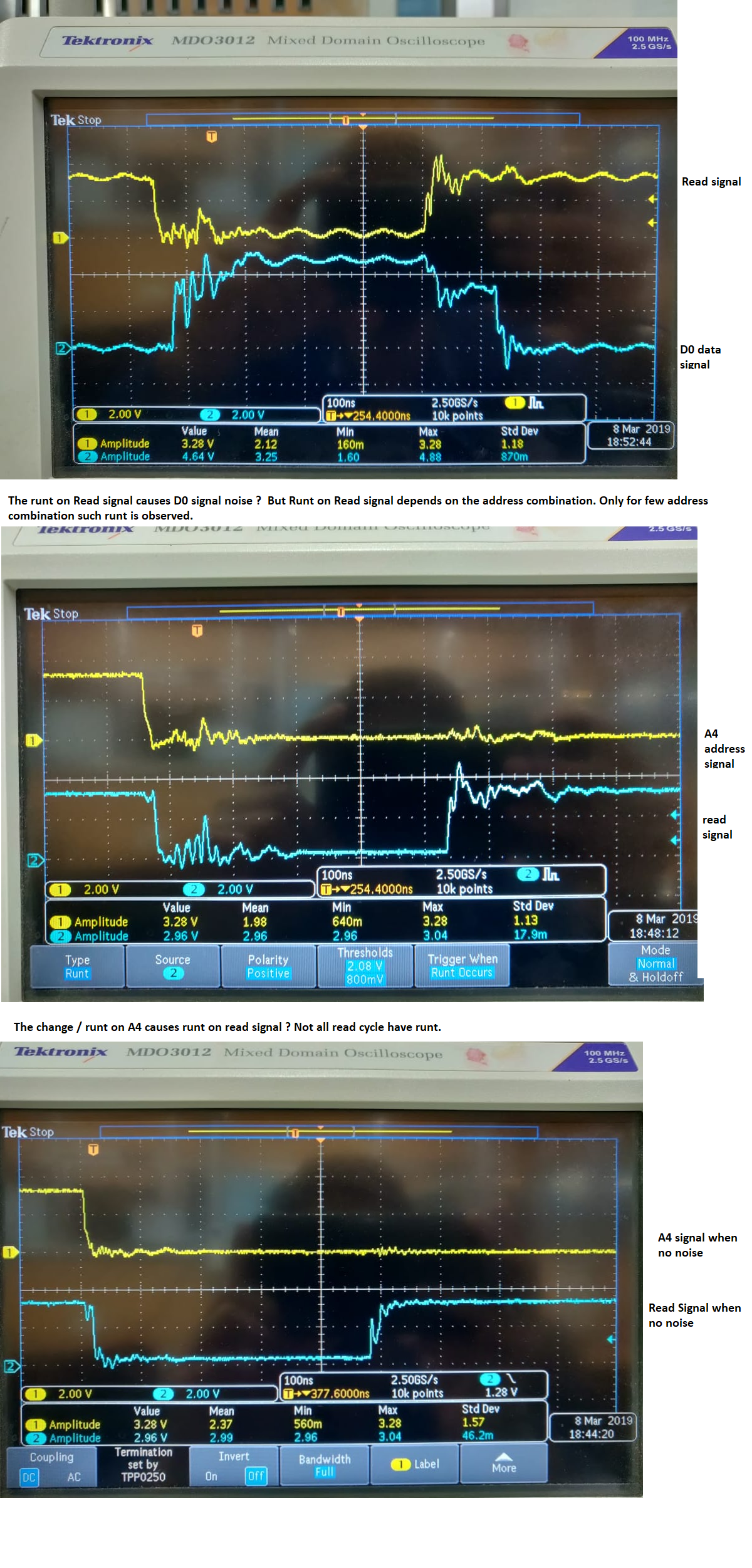
    What we noticed, is the Read signal and the Data lines are ringing, in such read failure cycle, which occurs, once in 20-40-60 minutes.

    The attached DSO capture, shows the read and data signal, get completely corrupted once in 20-40-60 minutes.

    This situation improved when we reduced the data lines pull-down resistors to 680 Ohms from earlier value of 10KOhm.

    We are observing the situation.

    When the 74LVTH16245 is disabled, will the floating input cause excessive current  drawn by this buffer ?

    Thank you for your patient reading.

  • Looking at the scope captures, I'm a bit confused.

    I see that the data line in the second scope shot increases to ~5.5V for a short time while the read signal is low.  Is this an expected behavior? Does the supply change during this time? The supply in the schematic is labelled as 3.2V, but the scope shot shows a pretty steady 4V signal -- is this also expected? The SN74LVT16245B is only rated to support up to 3.6V supply.

    Also, I noticed that the signals are extremely noisy, crossing the threshold voltage multiple times during what I assume is supposed to be a single logic LOW. Does this happen in conjunction with any particular logic state for the control inputs (OE and DIR), or is it random? Related to other data pin states?

    When the 74LVTH16245 is disabled, will the floating input cause excessive current  drawn by this buffer ?

    No - the input is not floating because this device has the H feature (Bus-Hold), which will hold the lines high or low, depending on the previous state when the chip is disabled. If you are using the SN74LVT16245 (no H), then yes, floating inputs would cause excessive current and possibly damage the device.

  • hello

    1. In the last observation the 4V signals were due to a pull up on the  74LVTH16245 to 5V.  We considered as these are 5V tolerant the 5V pullup should work.

    Now we have changed the pull-up to 3,3V signal and the 4V signals are no longer present

    2. The 5V on data signals you noticed is from our memory which is powered from 5V. This appears only during read cycle

    3. we find the read signal and address signals have ground bounce, which varies when the address , data combination changes.

    how to solve such problem

    We have one 74lvth16245 IC having a0-a15 lilnes, 

    another 74lvth16245 IC having d0-d7 [bi directional, using read control], a16-a19 and read, write signals

    Please find attached screen shots.

    Are these runts a problem due to power supply OR it is due to the 74LVTH16245, cause these two things are common.  In our system the d0-d7 buffer gets disabled one the read / write cycle ends. 

    We had attempted to make the power supply track very thick, added local capacitors of 100nf, 10nf ceramic, NPO type and also added 47uF tantalum with 1000uF electrolytic. None of these helped in making the Read signal clean.

    Where as the read signal is clean for many cycles, it gets corrupted only for certain combination of address / data change.

    We even tried to delay [60-80nS] the read low going edge, so that the address changes would settle down. However we noticed the read runt still occurs and gets shifted when the data is changing/ appearing from the memory.

  • Hello

    Here are few observation related to the runt on the read signal.

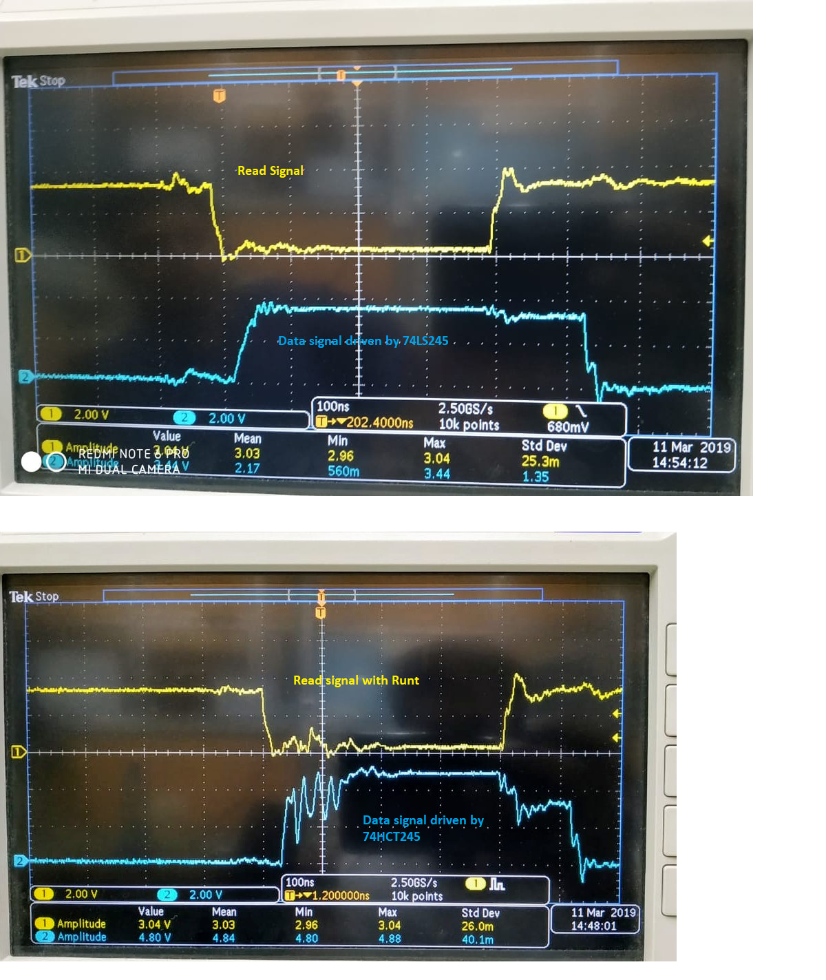
    we changed the transceiver on the memory cards, which were 74HCT245, getting activated on read low signal..

    These were replaced by the 74LS245.

    This resulted in A. reduced rise time of the data signals and B. removal of runt from the read signal.

    So the errors during read signals are removed and we could reduce the read width to ~200nS

    Here are two screen captures of same signals with LS245 and HCT245 both operting on 5V supply.

    What should we learn from these ?

    1. Are the 74LVTH16245 failing [as they share Read and data signals] ?

    2. is our power supply to 74LVTH16245 failing ?

    As such we can use the 74LS245 and complete this project, however we wish to understand the cause of failure to improve next time for a faster system.

    Thank you for the patience


  • Hi Namdeo,

    Emrys is out of office and not returning until Monday. Thank you for your patience during this time.
    The LS245 is a BJT device. It consumes larger Icc current as compared to HC245/LVT16245 device.
    I suspect that there could be some impedance mismatch issues going on too which might result in reflections causing spikes in the waveform. It could also be due to ground bounce( scopeshot of ground pins available? ) or crosstalk when other channels are triggering with some delay w.r.t to this channel.
    Also, I notice that you are using an older device (SN74LVT16245A) which is not recommended for new design. Recommend to switch to SN74LVT16245B and include a series resistor(25-30ohm) right at the output or close to the output of the LVT device to see the response.
  • You mentioned that you tried "termination from 220R to 10K". If that was a series resistor at the receiver, it would not have much of an effect because the impedance of a CMOS input already is approximately infinite.

    There is no application note specifically for the LVT family, but the LVC Designer's Guide (SCBA010) discusses several termination methods (beginning on page 1-27):

    […]
    Technique 2 results in a heavy increase in power, with no delay being experienced, and is primarily used in backplane designs where proper drive currents must be maintained.

    […]
    Technique 4 … is useful for point-to-point driving.

    Technique 5 consists of a diode to GND that should be located as close as possible to the receiver. An increase in power is not experienced, no delay occurs, and this configuration is useful for standard backplane terminations.

    Technique 5 is the most attractive of all techniques since there is no power increase and no delay occurs. However, since the delay associated with Technique 4 is so minimal and since no additional devices are required, whereas in all the other techniques at least one additional component is required, Technique 4 is usually the technique recommended by the Advanced System Logic department of Texas Instruments.

  • Thank you So much Clemens Ladisch

    We are using 74lvth16245A. we had wrongly mentioned 74lvt16245A.
    We tried technique#1 termination, and 220R worked.
    We also added series resistance in output of 33R to reduce the reflections

    What we find is that the 74LVTH16245, demands high current , when inputs are in between 1-2V. Causing some other outputs develop a changed VOL of 1-2V momentarily [20-40nS]
    Due to this high current the LD1117 LDO powering only the TWO 74LVTH16245 ICS, drops voltage by 0.4V [a ripple of 300-400mV lasting for 50-80nS]

    Now the system is working, but rarely at address xx00 [when a9-a0 = 00], the read fails.

    All along for last 4-5 weeks we find the failure is for combination of address data, where more signals change to 0.

    No amount of power supply track strengthening helped
    No amount of additional capacitors on IC pins helped.
    Attempted tantalum, electrolytic, ceramic 10-33uF and 100nF/10nF COG as well

    Now errors are rare, once in day, BUT we want to be sure of removing the complete noise, before system gets deployed.

    We have modified the 74LVTH16245A circuit and split it into two, by using 74LVTH245. This observation we will update soon.

    Thank you for the patient reading.
  • Hi Namdeo,
    Thanks for your post. The best thing you can do to thank Clemens is to mark his answer as the resolution to your issue (green button), which gives him additional points as a community contributor and let's people know that his post is helpful in resolving this type of issue.

    If your issue is actually something additional, you can always either reopen the thread, or click the "+ Ask a related question" button at the top of the forum to continue the discussion.