This thread has been locked.

If you have a related question, please click the "Ask a related question" button in the top right corner. The newly created question will be automatically linked to this question.

TXB0108: Problems driving TXDB0108 outputs with 3.3V CMOS

Part Number: TXB0108

Hi TI community,

I'm working with a design that uses the TXDB0108 to step up 3.3V lines coming from a Spartan-6 FPGA to 5V.

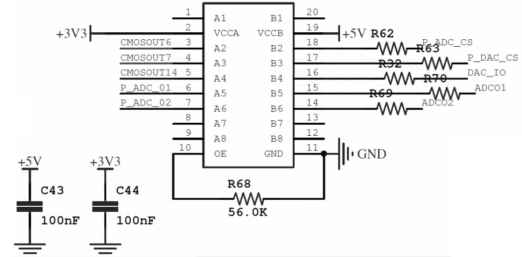
The pin-out is simple... with the GND pin grounded, and connected through a (56k) resistor to the OE pin. VCCA (toward the FPGA) is 3.3V, while VCCB is on a 5V rail. Finally, there are additional pull-up resistor on each of the logic lines coming out of the 5V side.

The logic lines from the FPGA are 3.3V CMOS. I'm able to apply these signals successfully to one side of the chip, but the corresponding line on the 5V side remains at 0V.

I know there are requirements for driving pins on the TXDB0108, so I'm wondering if I need to change someone about the logic lines coming from the FPGA.

Thanks a lot for your help,

Ian

  • Hi Ian,

    If you have scopeshots to show the input and output lines, it will be helpful.
    The OE pin should be connected to Vcca to be enabled, are you driving that line high or only having the 56k pulldown to gnd?
    I would not recommend having the external pullup resistors on the IO lines.
    Please read the app note:
    www.ti.com/.../scea054a.pdf
  • Hi Shreyas,

    Please see the following schematic diagram:

    Where the resistor on the output lines are 52 ohms.

    When I power up my device, VCCA and VCCB are to spec. I can apply a 3.3V to A2, A3, and A4, and B2-B4 will remain low.

    From what you described, it sounds like my problem is that OE must be tied to VCCA. Do you agree?

    Also, if I want to run A5 and A6 as inputs to my FPGA, will this configuration still work? (That is the function of a bidirectional level translator as I understand it.)

    Thanks a lot for the timely and informative response,

    Ian

  • Hi Ian,

    Yes, the OE must be tied to Vcca for enabling the device IO channel communication. Right now, the IO channels are all in Hi-Z.
    The TXB is auto bidirectional translation which can have A to B or B to A communication in the same device. So, yes, you may have the A5,A6 channels as inputs to FPGA with the others as outputs. you can also have the unused channels at gnd.