This thread has been locked.

If you have a related question, please click the "Ask a related question" button in the top right corner. The newly created question will be automatically linked to this question.

TXS0102: TXS0102 VCCB & OE pin design question

Part Number: TXS0102

Hi Sir,

My customer designed TXS0102 and the project schedule almost production, so the schematic & layout design can't be changed.

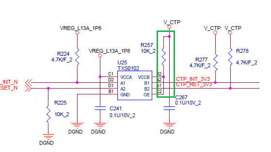
But we just found a wrong design in their circuit as below, VCCB & OE connect together through a 10K resistor to V_CTP shows as below.

Is there any way can helping on it? like reduce the R257 resistor value to meet VCCB & OE spec.

Or any suggestion, please let me know.

Thanks

  • Add one more comments for the power value, FYI

    V_CTP is +3.3V
    VREG_L11A_1P8 is +1.8V
  • Hi Anne,

    Its fine to have the OE connected to Vccb as the OE is overvoltage tolerant.
    I would strongly recommend against having pullups on the A/B IO ports. The TXS0102 has 10K pullup resistors on the IO ports by default.
    Let me know.
  • Hi Shreyas,

    Is it also good to have 10K ohm pull up in VCCB pin?

    could you please double confirm the schematic I provide below will no issue for application?

    please be aware the VCCB pin & OE pin design, Thanks

  • Hi Anne,

    OE to Vccb is fine. The 10k to Vccb will limit the Vccb current and response. It can be removed.
    Would the customer remove the external pulldown and pullups as well?
  • Hi Shreyas,

    Thanks for your explanation to make me fully understand the 10K pull up for VCCB will limit the current and response.
    So that's why customer said they make the mistake to design like this, and want to check with us,
    If they can change R257 to 0 ohm or any lower value than 10K are fine for their design? or any risk they need to take care? please advise.
    If any suggestion on their current design, or you think they must to change their design to make R257 to OE pin only and VCCB to 1.8V directly like below.
    If your comment is must change, we need to inform to customer immediately.

    Thanks

  • It seems that you are showing 2 different schematics here. R257 is not seen in your most recent post.
    this is I2C translation signals and I think what you have here is fine w.r.t Vccb and OE.
    I would also recommend to remove or DNP the R276, R275 resistors.
  • Hi Shreyas,

    Sorry for confusing you, and let me describe it more details again,

    What I mean is customer designed their board in figure 1, and customer said they make the mistake to design like this, and want to check with us, if they can change R257 to 0 ohm or any lower value than 10K are fine for their design? or any risk they need to take care? please advise.

    And for figure 2 is just an example that the correct design follow from our suggestion in other project, and just show an example that customer must design like this? Or customer can tuning figure 1's R275 value lower also fine for TXS0102.

    Figure1

    Figure2

  • Anne,

    Understood.
    My suggestion would be to remove the R257 10k and replace with 0ohm.
    and DNP (do not populate ) the R277, R278, R224 and R225.