This thread has been locked.

If you have a related question, please click the "Ask a related question" button in the top right corner. The newly created question will be automatically linked to this question.

SN74LVC1G74: abnormal behavior when using power bottom configuration

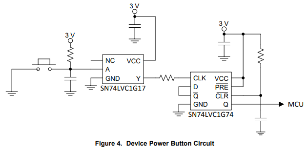
Part Number: SN74LVC1G74

Hi, 

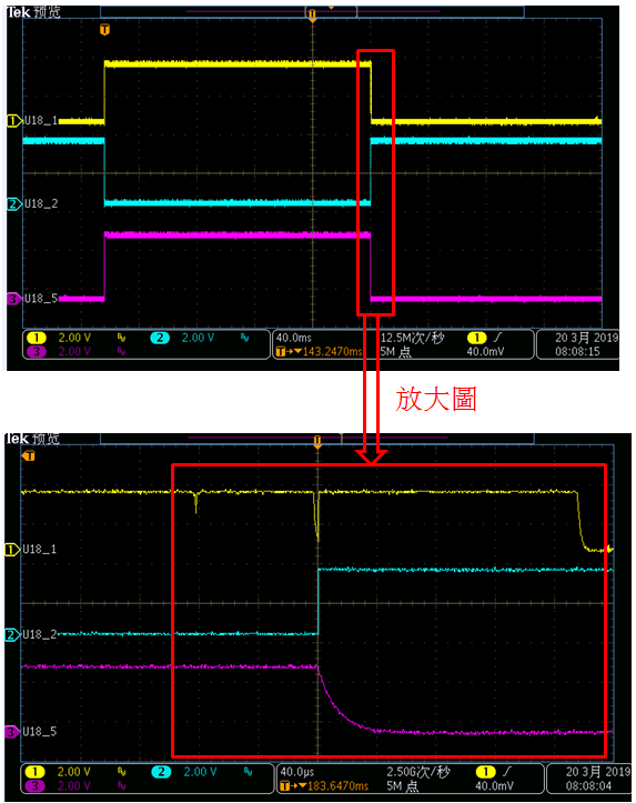
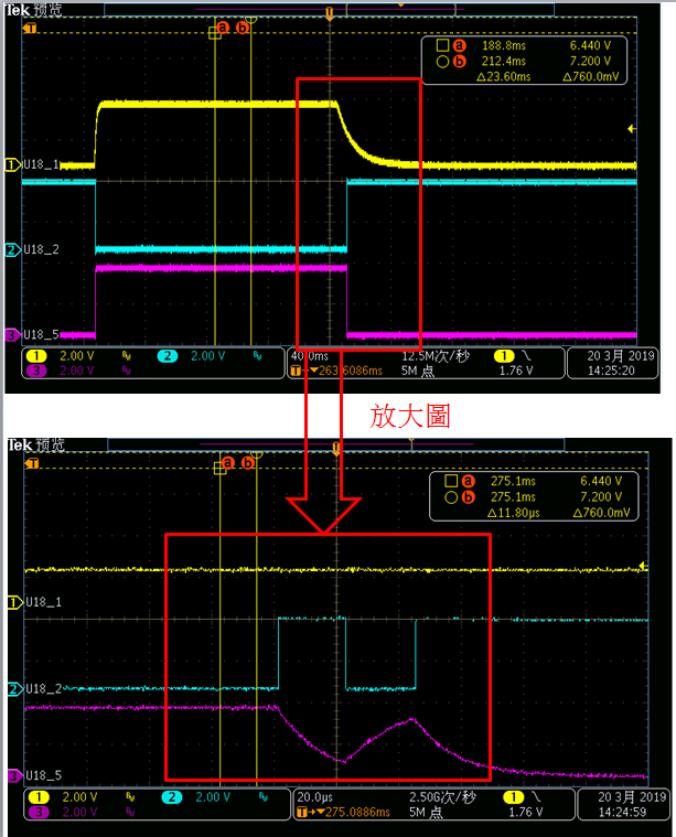
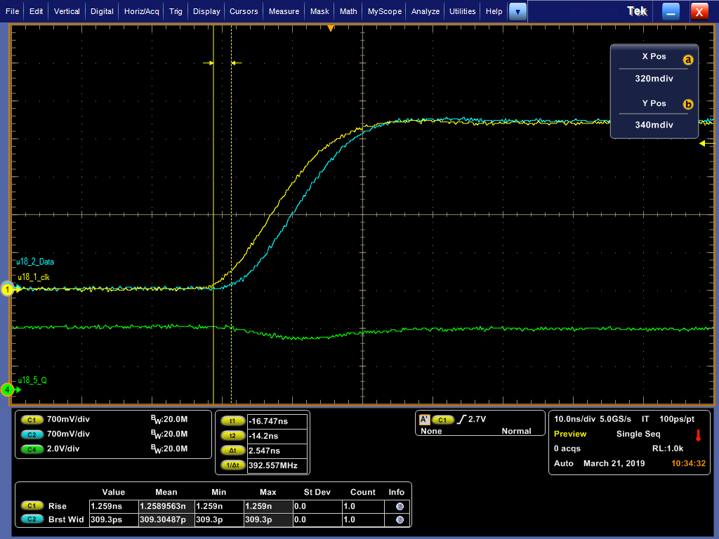
My customer is using this part for the power bottom trigger with below configuration, but even the clock is at falling edge, the output still change. 

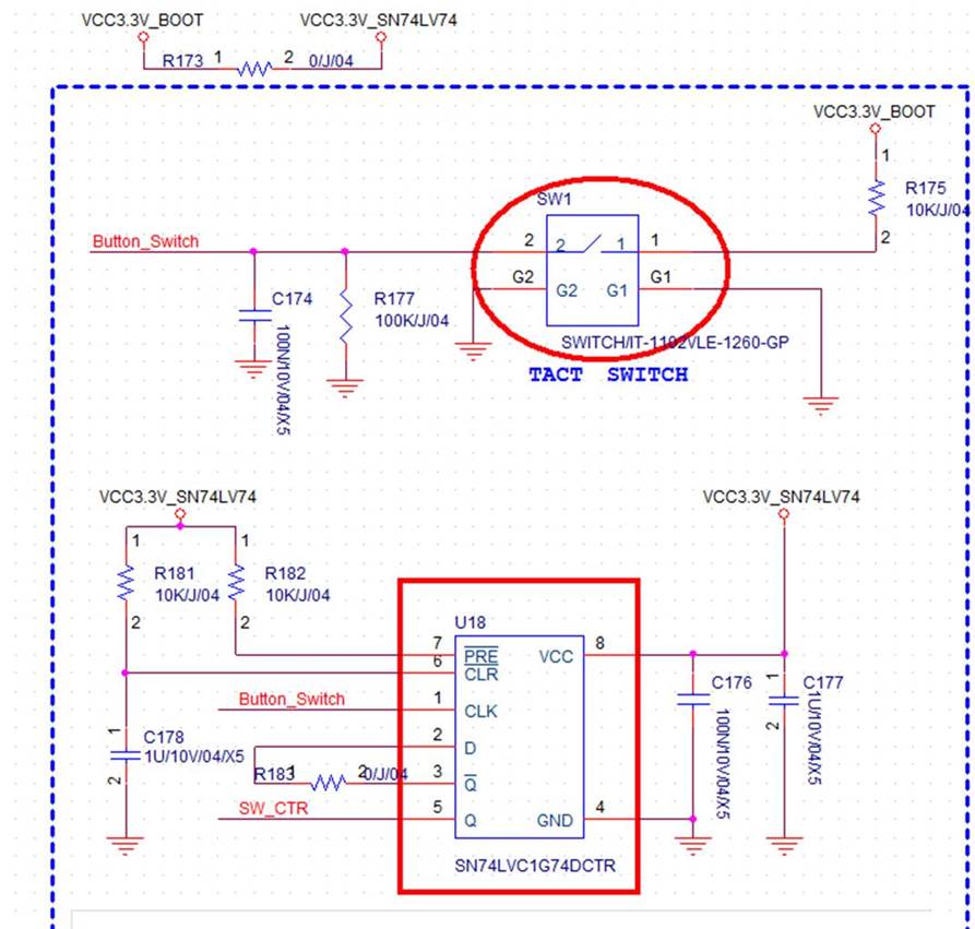
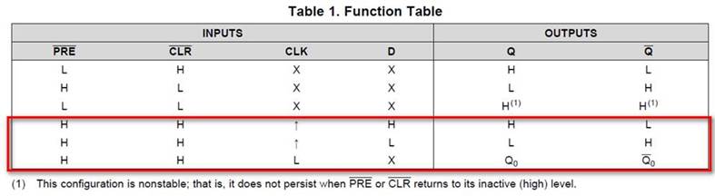
This does match with the truth table in the data sheet. 

Abnormal waveform shown below: 

Yellow: IC Pin-1 (CLK) ; Blue: IC Pin-2 (D) ; purple: IC Pin-5 (Q)

Please help to comment if there are modify needed of the configuration there are comments from your side how to deal with this problem and fix the behavior of this part. 

Thanks for your help. 

  • Hello,

    I would recommend looking _much_ closer at the edges of the signals. This device responds in just a few nanoseconds, so looking at a 1s/div scale really won't show you anything.

    I can see immediately that the CLK input on the SN74LVC1G74 is being subjected to extremely slow signals that need to be sped up for proper operation.  From the datasheet, here's an example of the correct setup using a Schmitt-trigger buffer to clean up the slow edge from the button debounce circuit:

    If this resolves your issue, please click the green "this resolved my issue" button, or if you need further assistance, please reply and I will continue to assist you.

  • Hi , 

    thanks for your reply and i will ask RD to test with the buffer to see if there are improvement on this issue. 

    after zoom in to the falling edge, there are some noise at the falling edge: (condition without C174) 

    but after putting the C174 back: 

    Can you help to comment why the output still changing even there is no noise on the CLK pin? 

    Great thanks for your help.

  • Do you see how the CLK signal appears to be a DC value at the 20us time scale?  This is why you are having problems.

    The datasheet clearly lists the required transition rate for CLK to operate, which is 10ns/V.  Your transition rate is much too slow, which causes problems for CMOS devices. This is a fundamental aspect of CMOS technology, and is the reason our application schematic in the datasheet includes a Schmitt-trigger buffer to clean up those slow edges.

    Here's an FAQ that goes into some details:


  • Dear Emrys

    We added a buffer between the button and the D Trigger in input.

    But the issue is still not solved.

    The input rise time is around 10ns/V now.

    As shown in the snapshot below, we noticed that the input signal(u18 pin2) rised with the clock rising(positive) edge simutaneously, without any delay;

    Similarly, it happens at the falling edge.

    Why did they happen? How can I avoid it?

    Thank you!

  • It looks to me like the output attempts to switch LOW when the lock triggers, but there is too heavy of a load on it. Two things come to mind:

    (1) The device may have been damaged from the previous use with slow inputs, causing a reduce output drive strength. I would try swapping to a new device with the updated circuit.

    (2) You may have to buffer the output to reduce the load.
  • Thank you, Emrys
    This issue can't be solved.
    Please give me some advises for value of the Res and Cap in "device power button circuit".
    I tried 3 pieces boards,
    one of them succeeded, while the other two still failed to sovle the issue.
    I notice that the caps round the IC is differenct(which was reworked), but I can't determine the exact value of the caps.
    So, do you have suggestions about the spec value of the caps, which were illustrated in the datasheet but without any spec value.
    Then I will try it again.


    Thanks very much
    Best Regard!
  • I believe the issue to be in 2 places

    (1) The inputs need to be buffered
    (2) The output needs to be buffered

    I don't think there's any problem with your RC values, at least not based on the first scope shots you sent. The RC circuit is efficiently debouncing the switch, but the edge is too slow for the input of the CMOS device -- which means you need to buffer the input with something that _can_ support slow inputs. (ie the Schmitt-trigger buffer I suggested)

    The output appears to be driving a relatively heavy capacitive load (you can see the slow RC curve in the 3rd and 5th scope shots on the page. The excessive load will keep the device from switching -- by buffering the output, you will allow the flip-flop to switch and the buffer will drive the capacitive load.